2010-12-31

New Year's resolutions...

This year is coming to an end and this will be my last post (this year). I didn't post as many times as I wanted (I planned once a week, I'm close to once every two weeks), but that's the way life goes.
Most projects are "work in progress", so these are in plan for next year:
  1. in the mini68k I wanted to finish a working gdb-stub before advancing to the CP/M-68K code. I finally managed to make it work, but there were some bumps in the way. The way ahead is not without it's perils, to use gdb and CP/M at the same time I might need an extra serial port for which I have no breadboard space. I'll need to draw the schematics, possibly make a PCB, make the SDCard interface work and then port CP/M to it;
  2. in the mini85 I wandered off in some hardware questions (casing, with a floppy or without, processor speed, with DMA, cheap DMA, video, expansion, connectors, front panel, size of RAM, SD Card, SD Card removable, Flash or Eprom, serial ports, parallel port...). I'll need to settle down on the hardware, draw schematics, make PCB, fit in a case and close it;
  3. in the Solarlight project I still want to fit it neatly on top of my Pepper pot and to tune some more code, also add a larger heatsink for the LED. I also plan to do a new SMD PCB and bake the components in a SMD oven. Further, I'd like to build a bike light with the same circuit but no solar charger. I'll need to get the final schematic, draw the SMD PCB for solarlight and bikelight and make the code linux-buildable and downloadable;
  4. in the SBC6120 project I'll need to decide on how to fit everything inside the box and fix the harddisk to the PCB, also design the front panel, back panel and connectors.
  5. in the home monitoring project I'll need to rewrite the code for the new light sensor and adjust the pachube data to it.
I don't think I'll run out of electronics projects for next year, but if just in case I do, I have to change a pedal crank on my Kronan (got bent on a recent fall on the snow) and I'm waiting for some studded tires :-) , read some more books and try to reduce a bit the coffee intake...

2010-12-30

gdb-stub for m68k quirks and tricks

After some investigation I finally realized how most of the gdb-stub works and how you can make it work, I also found out what doesn't work and that there are some things I still don't fully understand.
After having a stub that I could download to the target's ROM (in this case an EPROM Emulator) and would properly communicate to the gdb running on the host, I built a C runtime assembly file (crt0.s) and linker command to place the program in the available RAM. Since I had done a similar work for the stub running in ROM, it was only a question of changing some parameters and some basic code at the start up routine.
The test program was very simple, I didn't want to test any advance feature just a simple program flow with loops.

When I added a coded breakpoint in the code, all would work consistently, I could continue without a worry, control flow would be transferred back to the stub when the breakpoint was hit.
But as soon as I added a gdb break point what I expected to happen was, gdb(host) would read the contents of the instruction at the breakpoint and substitute it by a breakpoint opcode (TRAP). From reading the gdb-stub code and most internet references, a breakpoint should be a TRAP #1 instruction, I had setup the gdb-stub to intercept TRAP #1 instructions and report them as breakpoint to gdb(host), but every time I place a breakpoint I would get a privilege violation at the address following the one of the breakpoint.
The problem was that gdb(host) instead of adding a TRAP #1 (0x4e41) would add a TRAP #F (0x4e4f) (!!!), see it in the below:
I set a break point at line 20 of the code, gdb(host) tries a Z0 command but the stub doesn't implement it, gdb(host) acknowledges it, then it reads the code at the breakpoint position (m4074,2 with reply 2039), then writes a trap instruction at this address (M4074,2:4e4f).

You'll need to click on it to see it ok, sorry couldn't solve this one in the old fashion way..
When after several tries I decided to check "everything" that came in and out of the stub, I check that the instruction is in fact a TRAP #F and not a TRAP #1 as I was made to think, naturally I had not set the gdb-stub to catch these exceptions, then the stub would return to the address following the trap which is not an instruction, hence the privilege violation.
This problem above is probably solve in some gdb configuration line, but I didn't found it yet.. If I do I'll post it back here.
The second problem is only detected when you get these breakpoints to work. After the breakpoint the PC is pointing to breakpoint+2, before you continue you need to roll the PC back by two. This can be done either by the stub or gdb itself. I chose to do it at the stub, but it is possible to do it at the gdb(host) (also some configuration option must be there...). The only problem with any of these is that once a breakpoint is hit, it must be disabled before execution continues.
Gdb(host) just before you continue changes the instruction at the breakpoint address to a trap, then execution continues, when the breakpoint is hit control is given back to the stub and the instruction at the breakpoint is replaced by the previous. If the PC is rolled back by two, at the next continue, the same breakpoint will be hit without further processing... so we are blocked... An option would be to control everything from gdb(host), before continue, single step one instruction (the breakpoint instruction), change the breakpoint by a trap and then continue... I will have to investigate a bit further to see if this is already implemented in gdb but it seems (as Mythbusters would say Plausible).
If you are also curious about why the coded breakpoint (TRAP #0) above is different than the gdb-inserted breakpoint (TRAP #1 or #F) it is because gdb-inserted breakpoints must roll back the PC, coded ones do not.

2010-11-21

making gdb-stub work from rom

Well after some long break I'm back on the m68k... I had time to draw some of the schematics of the circuit, only the CPU and most of the support circuitry. The rest of the circuit is straight forward, I connected my EPROM emulator and a massive 512K bytes SRAM to the bus and finally a MC68901 Multi Function Peripheral (MFP) handling the serial port and SD card interface. The CPU clock is at the moment 4MHz, so I can share it with the MFP, later I intend to clock the CPU at 8MHz.
Since my previous post, I've done/settled on a couple of things:
  1. I'll use gcc and gdb to do get the system up and running. Currently I managed to compile gcc-3.4.6 for target m68k-elf and gdb-6.8;
  2. I've created basic linker scripts for running from ROM and running from RAM. Both have been proven to work with C source (C++ probably won't work). I've also created two CRT0.S for each of these linker scripts;
  3. Compiling the gdb-stub and link it to ROM proved a big challenge, but I managed in the end. The source m68k-stub.c that comes with gdb suffers from severe bit rot, most of the assembly source doesn't compile either because the syntax is no longer supported or because "handling multi line strings has changed in 2001";
  4. Still doesn't work perfect, the first time I load, break main and continue, remote-gdb ends up "somewhere", on the second time I load and continue (no need to break main, this is handled by the server) it works OK and I can even step lines of code. This probably has to do with my "trick" to make gdb-stub work from ROM without referencing any program at all (the frame information is not correct... I think...). On the second run (after the initial crash), this frame is correctly initialized.
  5. I'll add a 3V power supply and a SD Card interface for "disk drive", based on some previous work I did with the Arduino, I don't expect big difficulty.
  6. Placing the vectors in memory was actually quite easy, I needed to learn some m68k assembly and now I do it in CRT0.S. Due to a requirement of the gdb-stub to identify the generated exception, I had to build a two step exception processing. First the vectors 0 to 256 are initialized to unique locations starting at 0x400 in steps of 8. On each of these, 8 bytes there's a NOP and a Jump to Sub Routine long to the exception_handler, this pushes a unique address per exception on to the stack, the exception_handler pops this address and identifies the exception that was generated.
I had a old monitor that I "pop" from storage, to test dual head with openSUSE 11.2 and it works great. I really think it's a great advantage to work with two monitors, one for programming other for debugging or one for drawing the circuit and the other to check the PCB, Bill of Materials, Stocks, vendors, spreadsheet, etc.
Another thing I noticed is that I still can't get away from printouts of the code.. and I wish I had an old matrix printer with form paper... those were the days...

2010-11-13

Hardware Single Step for the 8085

As usual my current developments tend to wander towards all directions, as the ever expanding universe... Although I haven't really finished any of my other "side jobs", I want to further develop the mini85 into a real single board CP/M computer, but more on that later.
This week, I looked for a Hardware Single Stepping circuit for the 8085. Something that proves that "everything is on the internet" is not true (if you didn't already knew), at least until up to now.
The internet came up with nothing, so I had to resort to older methods... Books, applications notes, etc... First of it was the 8080 datasheet, on the description of the READY line it states "Can be used for single stepping the processor" but this sentence is strangely absent from the 8085 datasheet (a nice circuit with one wait state is drawn instead). Then I found something on a great book "Microcomputers and Microprocessors - The 8080, 8085 and Z-80 Programming, Interfacing, and Troubleshooting" by John Uffenbeck. There are caveats, about the same as others and my previous pseudo-DMA circuit for the 8085, doesn't allow the use of dynamic RAM hidden-refresh (end of M1). I've redrawn it with gschem.


It is not exactly what I want. I want a single lever switch with 3 positions RUN, HALT, SingleStep. I found this one on Digikey a nice C&K switch that "has the looks" of a 1980 Computer and could do the job. The problem is that I need to do some adaptation from the schematics above to a single switch with 3 positions, the main problem is halt the computer when the switch is off (centre position) and at the same time set the FF clock low... I might need some magic...

2010-10-28

SMD help

I sometimes boast about my old SMD soldering skills to my "happy hacking" friends... It's quite safe, until someone actually asks you to do _this_! Alex bought some of these JeeNodes from JeeLabs and needed some help. I accepted the challenge...
Before we start, a word of wisdom... Don't try this at home if you don't have the right tools, if you are uncertain about your tools or your ability it is best to send the module to JeeLabs and he'll repair it for you.
Following the site it is easy to understand the problem, Vout and Vin are connected to the wrong sources (this is a linear regulator Vout must be lower than Vin). The solution appears easy but it was not clear from the pictures, once the IC is in the vertical, there are two sides to chose from.
I usually start with the board to repair over a clean sheet of paper, makes easier to see as there's a better contrast, also if some small components come off the board or need to go in they're easy to see.
I then apply a small blob of solder to each side of the IC. The blob keeps liquid for some time and allows you to heat the other side (it must be a quick movement), once both sides have liquid solder slide the IC off the PCB to the paper.
Then using solder-wick clean the excess solder on the pads and on the IC feet.
I then marked the pads and the IC feet with the numbers and visualized what I had to do.
The IC actually is placed in "dead bug" style (but sideways), this means that the IC is "top-to-bottom", it is not so clear in the JeeLabs pictures.The mechanical pencil is 0.3mm for reference.
Finally I used some wire-wrap wire to connect the "floating-pad" to the board.
Since I have no idea how to connected to the JeeNode, connected it to the USB port and checked if the output voltage was around 3V... Some LEDs blinked (like in Arduino's FTDI), no smoke or hot ICs, I suppose it's fine...
SMD reputation intact...hopefully :-)
PS. - google.reader.friends if you have two posts one with pictures and other without pictures, it's just me and my faulty brain...

2010-09-03

8-bit single board computers

Before I build my own single board computer, I wanted to do a study of past and "present" single board computers that "could" run CP/M, focusing in their features and capabilities. Since I like CP/M-80 and I already managed to build a few breadboard computers that could run CP/M from a floppy or memory, I thought could build something more permanent.
Most of the SBCs I've listed below are for the Z80, or derivatives.
  1. SB180 (from Micromint, details published on byte Sep-Oct 85 designed by Steve Ciarcia) uses a HD64180 (or Zilog's Z180) with 2 DMA channels, 2 Serial, floppy interface using FDC9266 (for high density disks) (update, I've changed the picture and here there's even a SB180FX).

  2. P112 uses a Z182 with 2 DMA channels, 2 full serial and a FDC37C665 for floppy interface, extra serial ports, parallel port and possible IDE drive (PC-style super IO, includes high density) (new version was being sold here, apparently there wasn't enough critical mass).
  3. CPU280 uses Z280 with 4 DMA channels, 2 serial ports and a FDC37C65 does the floppy interface (also high density disks), although some details can be found on the internet I was unable to find schematics.
  4. N8VEM (designed by Andrew Lynch) uses a vanilla Z80, serial port with 16C550, huge SRAM 512K (mostly used as a RAM-disk), big Flash Rom 1Mb with operating system (CP/M) included, ECB bus interface, Floppy interface is an external board (new design, several boards and developers here), RTC and parallel interface (i82C55) and it's all open hardware.
  5. YASBEC also uses Z180 but the hardware details are much more elusive in the internet, the disk format suggests 3.5 inch HD drives.
  6. PROF80 uses a Z80, has a floppy interface with the UPD765, high density data separator, bit-bang serial interface, on the webpage there are more details ans schematics of other boards (graphics terminal) and upgraded version with Z180 (with FDC37C68, RTC and other goodies) some more details here.
I think after that review, I can settle on what I want for my CP/M SBC with the 8085. A 3.5 inch floppy (HD), 765 Floppy interface, 8085AH-2 @ 10.24MHz (2% overclocked) a 8256AH, 128K SRAM and 32KB ROM (with a debugger, Forth or Basic and boot). On the optional is a second serial port, a parallel port, a SD Card interface and an expansion port. I think I can skip the RTC as CP/M 2.2 doesn't need it and it's optional for CP/M 3.0 .
Front panel inputs I'd like to have a RUN/HALT/SINGLE STEP switch on the front, a RESET push-button and an interrupt push-button (maybe RST7.5 or TRAP). As for indicators a RUN/WAIT/HALT (green/yellow/red) LED, a INTR/INTA (red/green) and a HOLD/HLDA (only if there's an expansion port).

2010 "balcony carrots" grand cru

For those of you that just arrived, this blog has nothing to do with wine... today I'm talking about carrots. This year's crop of carrots from the balcony vases was about 200g, slightly less than last year's (300g), but I planted other stuff (some worked out, some didn't). Crops were delayed (about 1 month) this year due to the harsh winter. We also had a new arrival, little Luísa! She loved the carrots as finger-food... extra tasty!

She is now 9 months and moving around, she takes much interest in my books...

But most of the time she's a sweet baby...

2010-08-18

Mending Jeans

I bike to work regularly, even during winter. As a result my jeans wear off often, every time in the same place, let's call it "the saddle area". I used to take the jeans back home and ask mum to do it. She would just go to her "work room" power up her good old sewing machine and get it done in no time.


Since we decided last year to buy a sewing machine, I thought I could try and do it myself. It is very easy and hardly noticeable once the patch is made.
You will need a pair of jeans to fix, a jeans patch a bit bigger than the hole (+2cm, 1 inch) and thread.


There's a trick about the thread (thanks mum), use grey or light grey thread. Using blue thread, even if it's the same colour as the jeans will produce a noticeable patch.


Place the patch on the inside of the jeans and secure it with pins, take care to stretch both the jeans and the patch.


Load the top thread with the grey coloured thread (the under carrier is not so important), select a wide zig-zag stitch (5mm width) and reduce the length (advance) to 1 to 2mm (a bit like the bottom right stitch of figure 2 here).
Lock both fabrics under the zig-zag presser foot starting from 2cm/1 inch outside the hole to cover, sew until 2cm/1 inch the hole end. Repeat in reverse.


When you reach the place where you started, move the needle to the top most position, release the feet, move the fabrics 5mm (about the width of the stitch) to the side, press the feet and repeat until the hole is covered.


Here is the patch finished. The good news are it is hardly noticeable, the bad news are, that usually if you do this in one leg, chances are the other leg's fabric will also fail in a few weeks.

2010-07-06

Prototype PCBs with Toner Transfer

I wanted to redo my old Munny project and build a new versatile PCB that had a minimum ATTiny15L system with in circuit programming (ICP). I planned the RGB LED and the temperature sensor to be soldered on the edge of the board, like having solder tags. The rest would be the CPU, the programming connector and the minimum number of components (a few resistors and a capacitor).
Although I've already managed to use gEDA to design and send a PCB for fabrication, I wanted to try going "DIY" and have a faster "turn around" from project to board. The board would also be very small (about 2cm²) the cost of making a production run wouldn't be cost effective.
Before I've used the UV light transfer with very good results, even for double sided boards. This time I wanted something even more "barebones" only the etchant, no other chemicals (like the extra developer in UV photographic method). I found some sites with the reference to Toner Transfer Method. They used either inkjet glossy photo paper, a specific "Press and Peel" paper ending in common "glossy magazine" paper, there's even a nice page at Make: web discussion . I decided to give it a try!
First I designed the board single side only. I started out with 10mils/10mils/0.8mm (10/10 means 10 mils tracks and 10 mils minimum spacing between copper, a 10 mils is 0.01 inch; the last number is a minimum drill), but soon I had problems connecting the ICP with the defined tolerances. I changed to 6/6/0.8mm and finally managed to connect everything and pass the DRC test. The next step is printing.


My printer is a HP laserjet 4L (its old, 300dpi but it works!), it still has some problems that I didn't quite worked out yet. There is some rendering on the edges of the lines that I didn't managed to "clear out", I think it is the REt setting but I didn't managed to disable it with my linux driver (the printer is network connected), this is something I would like to solve. It might be visually more appealing when printing normal graphics, but for this particular purpose it doesn't work! Here's a picture of the zoomed output.
As you can see the horizontal lines (in the photo above, to the printer they're vertical lines) and edges have a "saw tooth" on both edges. As I said before I think it is a rendering/dithering that the printer "self" does to make the lines more eye appealing or it is a misaligned mirror.
I tried out 3 different types of glossy inkjet photo paper from Dutch shops. Bellow the three different papers ready for cutting and ironing to the board.


I obtained the best toner transfer with the HEMA glossy photo paper, not bad for the cheapest of all the options...

The transfer was clear and sharp... all the rendering artifacts appear in the copper. The paper that doesn't show has peeled off easy, the part that is attached is the one you have to scrape.


The first from the left actually when it transferred to the copper the toner transferred fully but in some areas it got stuck to the paper. It might mean that this paper need more ironing time, temperature or pressure (or all of the above)... I might try it again... the one in the far right is the HEMA paper, needs more scraping but the toner sticks to the copper fully.


This is the view of the most troublesome area, two wires going between two pins of the ICP and one track between pads of a SMD resistor, both around 6/7 mils clearance. I had to puncture the centre of the pins because I forgot to set "drill" in the print out and it helps a lot for drill bit centring.
I actually had to separate the track from the SMD left pad, the etchant didn't go through the little spot of paper (visible on the picture above). The picture bellow I removed the toner and performed an electrical test with the multimeter. I also drilled the connector.

After that stage I soldered the components and had my board running after a couple of minutes. Here's the final result. The power connectors below the board have been soldered for testing and programming, I'll be removing these... I'm also planning some tests and improvements to the board's software.
The connector ICP is a 6 pin female because it has a smaller (in height) footprint than the male connector. I'm quite please with the LM35CZ and RGB LED footprints, for such a small projects edge placement is viable and saves board area.
Getting the 6/8 mils was a bit of an over achievement and it is only viable because the board is small and hasn't got many connections, 10/10 mils should be the standard. I also need to see if I can solve the rendering of the printer problem... maybe (God forbid :-) using a Windows driver?
The soldering was done by hand and normal soldering iron, a "next step" would be an SMD-oven.
Tah Dah!

2010-06-05

SBC6120 - Casing (II) and power supply

I finally got my hands on the power supply of a _DEAD_ External Hard Disk that suited the purpose of powering my SBC6120. Before I was using a Compact Flash to IDE adaptor and I only needed a 5V supply but I wanted a "real deal" IDE drive.
My first try was an old drive I had around, a Seagate 89MB... unfortunately another case of R.T.F.M., disks with CHS addressing (cylinder, head, sector) are not supported, only the (relative) recent LBA (logical block addressing) are. Alex gave me a 3GB drive he had "hanging around" somewhere in a box, probably more than enough to hold all the source code ever produced for the PDP-8... It fit the case, just... probably too "just".
I still need to pack inside the case: a switching power supply (LM2575, two big caps, a diode and a fat inductor), the power connector, the IDE ribbon cable, the serial port connection, the power switch and (if possible) one or two front panel indicators (power on and disk activity).


The Case is a Hammond I bought some time ago for this project, but I never found a suitable power supply. Now with the external 12V supply and (this is a forward reference) the toner transfer PCB method, I can build a middle PCB board holding the hard disk, the CPU board, the switcher power supply (12V to 5V) and a power switch. I'm looking for switches like the one above, but I still haven't found a good right-angle-PCB-mounted... I'm looking at some lever switches from C&K, they look the right "age" for a pdp-8 simile. but will see what I can get my hands on...
Space in the box is tight so I still haven't decided where to put the power switch an a power LED, or if I just make some openings in the front panel and extend the LEDs on the board... I'm also looking for some front and back panel design...
There's a lot of mechanical engineering ahead... I love the smell of a challenge in the morning...

2010-05-28

Arduino interface to SD Card

Finally managed to interface to a SDcard to the Arduino. There are several "tutorials" and even libraries written for the Arduino, but my objective was not to use any Arduino library or specific feature (like the integrated SPI port), otherwise porting the code to the mini68k would be more difficult.


I started with this example (this other seems easier) and then started "removing stuff" in order to fit my purposes. I only need the basic initialize, read sectors and write sectors. In order to boot and run CP/M from an SDcard I don't even need to read/write more than a single sector as CP/M reads/writes only one sector, furthermore deblocking (breaking up a 512 byte sector into 128 byte CP/M sectors) is easily managed by most CP/M flavours (CP/M-80,CP/M-86,CP/M-68k, CP/M-Z8000).
I battled with some Arduino functions, I particular serial.print() functions. I'm suspicious that something doesn't quite add up, some of the lines of text that should be printed are skipped for no apparent reason. It could be by the fact that I directly access the port pins (DDRB and PORTB) but since I don't change the serial pins there shouldn't be a problem...
After several tries I managed to write and read a sector of the flash.

The hardware is at its simplest form, it is a basic resistive divisor by 2 for the card inputs CS, SDI and SCK, the SDO output from the card is connected directly to the Arduino input pin.
Pins CD and WP are also connected directly, the card detect(CD) and write protect(WP) switches use a weak pull up feature from the micro. A low voltage drop regulator provides 3.3V to the card.
I used the Sparkfun SDcard adaptor, but since the "freeday disappointment" I promissed never to buy from them until the EURO is >= 2x the US dollar (from that point on I would be stupid, not stubborn). The circuit used is the one of the first example above, except that I didn't bother to have the correct 3.3V input, I decided to go to 2.5V as it is easier to obtain (two equal resistors) and the input tolerance of the SDcard must accept it correctly. Usual (CMOS) input levels are at 60% (2.2V for High or 1) and 30% (for Low or zero) of Vcc (of the card).
Now I only need to port the code to the 68k...

2010-05-01

HDSP-2000LP Arduino

A few years ago I bought some 4x 5x7 small LED displays in eBay. I though they looked really cool to be used in a front panel display, instead of using a single line LCD. The datasheet was actually easy to find but driving the display...well that's another story.
The initial objective was to incorporate these displays as front panel to the mini68k, as usual I try to prototype it with the Arduino. It ended up as being quite hard, you must compose the characters as "bitmap" graphics, then shift the 24 bits for "column" one of all the displays, then activate column one for 2ms... then repeat to column 2 to 5.
So first you must compose the combined display bitmap from the individual characters, then shift a sequence of bits and activate the respective column. To do it proper you must have in memory a bitmap for each character, compose the "screen" and the shift the bits and activate the columns in sequence.

As you can see from my first program... it didn't go well... unless you're the Predator and your personal nuke is counting down...
A few more head bangs against the wall et voilà...

Finally insanity takes over and I try to do a space invader... (the following photos are so crappy I forgot to get out of the light shade, late night)

inter character spacing is too wide to make multi-characters symbols (like infinity) unreadable... let alone the space invader that got cut in half... probably from a missile F-111...

The code is here, enjoy...

2010-04-17

New Pachube Feed

I finally had the time to create a new pachube feed and add the humidity monitor. It was almost "plug and play", I only had to convert the float values to integers and then scale them for one decimal point. My webpage server program uses the server.print function and it doesn't accept floats as input.
I kept the Light sensor, so one can see the relation between the changes in the values of temperature and humidity with the daylight. Other interesting (and expected) reaction is the increase in humidity once the clothes were out to dry in the living room (as I did this morning) :-).


The sensor is powered by a microcontroller port, and it is not (yet) filtered, I'll add a small capacitor to the power pins. This would allow to power the sensor only "on-demand", but I'm not sure if there are implications on the sensors stability. I know that it needs some time to correct the humidity readings...
The speaker is used only to beep every time the Arduino is queried, it beeps every 15 minutes by pachube.
The code is here, the pachube feed is here, and the picture of the system is bellow.


2010-03-22

mini68k adding libraries and serial port

I admit I haven't been very focused at my hobbies, but that's life. I've been working here and there: getting the Arduino and the SHT11 working together (see here for library), converting a metal-gear servo to continuous rotation (I followed this how-to), trying to design a photodiode amplifier (I'm following this, this and what is available from this), debugging the SolarLight project and working on the schematics of the mini68k and finally getting some code running on it.
I've been feeling a bit more confident with gcc-m68k and I've been increasing the complexity of the programs. I managed to link in the gcc library (libgcc), I tried out the -msoftfloat option (compile, I didn't check the results of a floating operation yet) and I created my own putc and getc functions using the USART of the MC68901 (MFP) in pooled mode.
I want to change my CRT0.S to include some hardware support functions before main() is run. Initialize the interrupt vectors (pointing to a "interrupt error" routine), printing some console message during initialization and doing some hardware test (RAM, MFP).
I'm still unsure of a few things:

  • An interrupt level 7 is basically a NMI, my system switches from ROM to RAM at the 8th clock, at the 9th clock if a NMI is pending the CPU will jump to an uninitialized vector! I must read the specs again but I think this could be a problem. Or not, if the system is int7 incapable (IPL2/0 or IPL1 permanently to 1) or has a gate enabling interrupts;
  • the MFP interrupt is physically enabled (i.e. connected to the CPU or gated by self for example)? (see point above), how does gcc link to interrupts (newer gcc versions work well ex. AVR-gcc), how do I place the vectors in memory?;
  • I want to build a gdb-stub/rom monitor, will it handle the vector allocation/writing? If so, my operating system (loading from somewhere ROM or disk) will also be in supervisor mode? (and also handle these?);
  • Can/Should I implement some sort of memory protection (writes to first 1K-vectors and last 1K-SupervisorStack of RAM must be made in supervisor mode)?;
  • For the end project of a CP/M 68k what type of media do I use? Going back to floppies would be definitely cool but I'm sure I would need some sort of DMA as I don't think the 68000 is fast enough (and surely not at the current speed of 4MHz). With SD I'd use only a few I/O pins (from the MFP?) but some SD cards are only 3.3V and my system runs at 5V. Or I could use a Compact Flash card, most can work at 5V, and it is easy to get some old CF cards (64/128MB) or even a IBM microdrive I've found once here; I would need to build two 8bit ports (A output to control the drive, B for bidirectional data) and this is breadboard space...
  • I would also like to "upgrade" the logic circuits to one of the M4A5-32/32 I've build an adaptor for and change the DTACK circuit to actually drive the line when releasing the bus (until AS goes high).
Well for now that is a still a lot of work in progress, I doubt Spring and/or Summer will allow me more time but I'm trying to keep you posted.

2010-03-07

Arduino OpenSuse 11.2 (LED as light sensor)

I need to use my Arduino-shield-Breadboard for another project, so my Pachube-feed will be offline... for a while...

Next time around I'll add some more sensor that I have, like the relative humidity sensor.
I took the time to upgrade to the new Arduino-0018, here I encountered some old and some new problems.
First I needed to add my user to the dialout group in order to have access to the serial ports, as reported here (see last post). The other problem was an old problem, with the standard avr-gcc distribution of OpenSuse you can't program an ATMega328. I didn't solved it right now but the how to is here. But for now pachube is off-line (correction: is on-line but data is bogus).

Alex has a problem with his home monitoring system, he wants to monitor the amount of Water he uses by counting the turns of the pointer in the meter. He intends to use photo-reflexive sensor like this one.

Trying to help him, I started with using LEDs as sensors, Photodiodes are expensive and photodiode amplifiers difficult to build due to the very low bias current of the amplifier. My best results were using a IR LED as a sensor, but I'm still not sure if it will work with the set, in particular becase the sensor Alex has is a fototransistor not a photodiode, the principle used could be the same but instead of a reverse bias (anode to ground), the foto transistor must be actively biased (emitter to ground), the parasitic capacitor should still be discharged function of the light.

A good source of information is here, and here, I based my code on the Arduino example but I changed the port programming instructions for direct port access instructions (DDRD, PORTD), it is not "elegant" for several reasons but it is a bit faster and gives better results at high light levels.


The available pre-compiled avr-gcc does not allow you to program the Arduino Diecimillia (ATmega328 is only possible to do assembly, no C or C++). So my update of the Temperature monitor will have to wait...

2010-02-27

Das Blinklicht with gcc-elf-m68k

The first program you write when you learn a language is the "hello world" classic, in a embedded system where you don't have a serial port (or you don't know if it is working) you have to use "das blinklicht" example. Er... it's just a blinking LED.
After setting up the cross compiler tool chain you'll need to set up the linker script and the crt0.s files.
The linker script defines where (in physical addresses) is the RAM and ROM of your system, which sections of code go into where and in my case the reset vector and initial stack pointer. There are still some things missing (namely libraries, floating point and multiplication/aritmetic), but I'm a step closer. I must admit that I found these (crt0.s and ldscript) on the net but I don't remember where or who did them. I've just change them a little.
Although the ROM is mapped on reset during the first 8 clocks at 0x00000, after the 8th clock ROM gets mapped at 0x80000. When you are programming a real eprom (or using my "linux-updated" rom emulator) you must move the code to the bottom of the ROM. This is accomplished with the command "AT".

GCC creates a section of code for "initialized data" called .data, this section is put into ROM and at the start it is copied into RAM (at CRT0.S), with the blinklicht program I don't use any .data or .bss or even stack, so for now I will not test if this works.

Without using optimizations -O2 your software loops will not be cleared by the optimizer, and it is pretty easy calculate the time taken for the software loops.

I had calculated an access to the MFP m68901 every 15us with a 4MHz clock and what I had was 30us.. I found the "problem" the next day, the instruction timing sheets are for the m68000 with its 16bit data bus, a 68008 takes two memory cycles for each of m68000, therefore twice as long.
The simple makefile is here

SolarLight (7) - Software, AVR assembly


Ok, finally google docs supports any type of file so I can post all the project files in one place: code, gerbers, gEDA design files and spreadsheet with the calculations, requirements. It is all here.
I decided to try out pastebin, so I'm updating this post with the code for everyone to take a peek... In this version I'm still working on the "when to turn on" routine, I think it still doesn't work as I initially intended... pastbin doesn't look so good to paste long assembly lines, but here it goes anyway..

The software as it is now is working, it has some problems and "room for improvement" but it is working! You know the motto: Make it work, make it better!, make it faster!

One of the improvements would be to limit the time the light is ON to about 30min-45minutes, this would allow the battery charge to progressively increase during the good sunlight days and progressively decrease on a sequence of bad sunlight days (as in this year for example).
Other improvement could be a full darkness detection and adjust a 12h no light clock from there. It has happened that during the day when a big cloud (and/or heavy rain/heavy snow) the measured light level goes down to the "night" level, then if there's enough battery the light turns on... it shouldn't and I'm sure this winter is exceptional, but the only way to prevent this is to detect the lowest darkness point and count 12 hours from there, and only from then on the light would turn on when it is dark.

In the code I added a debug routine that is included when the two variables are uncommented (DEBUG and DB_CNT), when I wanted to output a value I load it in the DEBUG variable and call dbug. The byte is output in the status LED serially MSB first, there is a long (2 cycles) high pulse followed by clock and MSB data, clock and bit 6 data... clock and LSB data.

Finally my biggest problem was the branch instructions, the AVR has the following:
BRLO - Branch if Lower (UNSIGNED)
BRLT - Branch if Less than (SIGNED)
BRGE - Branch if Greater or Equal (SIGNED)
BRSH - Branch if Same or Higher (UNSIGNED)
I was not used to have these complex branch instructions, I'm used to Zero Flag set, Zero Flag Clear, Carry set, Carry clear... I'm specially not used to having a different branch for signed or unsigned... So I chose wrong.. result the jumps were not taken when they should. The ADC values are unsigned when read (0..255) but if you start calculating with them you can get signed (negative) values and then you have to use signed instructions.
AVR assembly programmer beware!

A final word about the Code, it was assembled with Atmel AVR Studio Assembler (Win), it doesn't output the number of cycles per instruction... a bit of a let down... :-)
And with this post I finish this project.... Woo Hoo!! Project is dead, long live the new Project...

SolarLight (6) - PCB Fabrication and Assembly

Using gEDA for producing gerbers turned out to be easier than I thought.
Recently the gEDA project has been under fire in slashdot due to its "complicated", "non intuitive interface" and lack of documentation. I really don't think that the documentation is that bad, it is scattered but it is not bad, just look here. I haven't meet an Open Source project that didn't suffer from the same problem, even (and particularly) the GNU tools. As soon as you get out of the mainstream gcc/gas/ld/gdb you're almost on your own, searching bits and pieces in the internet. Some of the best GNU project documents have been written by a commercial enterprise (either redhat, cygnus or other).
I call it Anarchic-Knowledge (or Anarco-Conhecimento in Portuguese), everyone omits to write what he finds trivial, forgetting that what is trivial to him, might not be for the community that will use the product. Then a plurality of tutorials, blog posts and guides show up, each one showing how they did it "their way". A new user has to pick all these pieces, try more than one and finally write a "I did it my way" post... And we all learn from this experience.It is not the lack of documentation, it is just the way that Open Source grows.
Back to the how I did it... :-)
I followed this tutorial, I had a single page schematic so it was easy to generate the netlist. I created a single project file with the schematic libraries, I used my own symbols since not only I wanted to learn how to do them but also I had a MOSFET with two Drain Pins that I could use each in an independent circuit. I used shell scripts to get the job done, I tried once a Makefile but I realized that I would have to change the Makefile for every project (even smaller ones), a shell script can do that at invocation time.
I also created some Footprints for my project (also for educational purposes), I had them in a library directory and used jcl's gnetlist invocation but with my directory instead. PCB must also be configured to have a pointer to your library in the "File-Preferences-Library".
First follow what gschem2pcb tells you to do, open the file, import the parts, spread them and execute the command, then I put in most of the mechanical details, using the outline layer in a place where no components were place, size of the board, cuts, groves and fixing holes. Also check now for the DRC tolerances in the File-Preferences Menu.
Then the fun begins, it is a very iterative process: place, route, looks good? can I do it better? with less vias? other mechanical problems? heat sinks/problems? repeat until satisfied with the design.
Then I place some more information on the silkscreen, plus signs on the connectors, output indication, board reference, moved the references so that all are visible when the components are soldered and facing the same side (so that you don't need to rotate the board to read the references). I also place on the top and bottom layer a square with the layer number inside, so that you can identify the layers on the gerbers and on the boards.
I was going to use Olimex pcb prototype services for my first gEDA boards so I needed to limit the number of drill sizes, they have some drill sizes that are considered standard and any other is considered extra (and you pay more), luckily someone from the gEDA-user group already made a drill mapping file for Olimex after executing the script run DRC again! Here's my final PCB result.

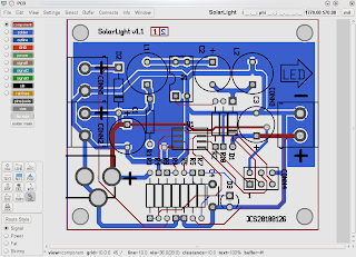
You can also export to png the two sides of the board in a "photo-like" picture, some people claim it gives better reading and it is easier to spot errors.

If you have no errors in the last DRC you're ready to produce your gerbers, and this part is as easy as pressing the correct button in export. Then with gerbv, check if the gerbers look nice and the drill sizes are correct.
Recently a good question came up in the geda-user mailing list, it sums it up nicely but the first reply reminded me of something I didn't do and should have done...
Print out your surface copper layers and put the parts on the printout to make sure they match.

yup, I designed my resistors with a 1/8W in mind and then I couldn't find any I had to use 1/4W.. so the resistors didn't fit in place. My DIP 4 for the MOSFET also didn't had big enough holes, apparently International Rectifier didn't stick to the normal DIP drill sizes, probably due to current capability or thermal conductivity. In that point, with some hindsight, I would increase the copper area connected to the drain, that could be a good heat sink for the MOSFET. I also should have thought a bit more on how to fix the board to the pole, with the new batteries the SolarLight is much heavier, I should have devised other way to fix it. Here's the board in place, note the resistors in two layers.
UPDATE: The resistor that is hanging and has two sockets is the gate resistor of the MOSFET, if you check the spreadsheet with the calculations you can see that the gate current has great influence in the MOSFET power (losses), so I made it low enough to still allow programming easily (now at 100R). When programming the micro the light turns on, but without any damaging effect as long as the frequency (of programming is high enough 250k) and the pattern is sufficiently random (see here for a bigger problem with ISP port sharing).


One last remark, if you buy microcontrollers in ebay and they say "New, Old Stock" it doesn't mean that they are not programmed, they can be factory programmed and that doesn't mean that they are not new! In case of the ATTiny15L, the low voltage programming mode can be disabled by this factory programming, if you solder it to the board you'll not be able to reprogram it. You need to remove it from the board and use a HVProgrammer like AVRDragon for example. Learned the hard way...