Showing posts with label electronics. Show all posts

2013-03-24

HF on the ATtiny15

I wanted my class E amplifier to be driven by an Attiny15. The idea is to build a HF (6.78MHz) low voltage and low power beacon.
The maximum PWM frequency attainable using the factory OSCCAL value, and using OCR1B=2 and OCR1A=1 is 8.525MHz with the only possible duty cycle is 33%. With OCR1B=3 we get 6.393MHz, OCR1B=4 we get 5.115MHz.

I want to use my beacons in the ISM band of 6.78MHz so the second value (OCR1B=3) is the closest. I managed to output a duty cycle of 25% (OCR1A=1) or 50% (OCR1A=2), this is perfect for a class E drive as 50% is available. The final tuning was done with trial and error on the OSCCAL value until I got the correct frequency.
In my tests, the factory value for OSCCAL (of all the Atmel Tiny15L I tested) would get you within 1% of the nominal frequency 1.6MHz, but with frequency measurement and tuning I got to within 0.5%.

Did a couple of other idiot measures and observations.
- The program memory of the ATtiny loops, the PC is only 9bits and when the last instruction of Program memory is reached execution continues for 0000.
- A NOP consumes less current that an rjmp +0, not significantly but noticeable. I fill the memory with each instruction and measure the current with or without BOD. The second instruction also take double the time of execution.

RJMP+0,BOD - 3537uA (AVG)
RJMP+0,NO BOD - 3494uA
NOP,BOD - 3503uA
NOP, NO BOD - 3458uA

- OSCCAL after reset is cleared and the measured clock frequency is 1.1MHz, when taken to 0xFF the frequency is 2.083MHz.
- Clock jitter of the oscillator. I filled the program memory with the following:
lp000:
.rep64
sbi portb,portb1
cbi portb,portb1
.endr
rjmp lp0000

I would then trigger the scope at the low level at the end of the loop. This gap would last longer than normal, then it is easy to trigger on it. You can just see it under the trigger arrow in the picture above.


I would the trigger to the flank increase persistence to max and let measure. the jitter.


The waveform goes up quite fast (in less than 10ns) with the oscilloscope probe as load. With a gate of MOSFET... it's not so good...

2013-03-02

Class E - selecting a switch

After the initial results (with a simulated ideal switch) here, had to design a real circuit. Having seen a lot of projects with the 2N7000 and having a few in my surplus bin, I used it in the simulation.
Finding spice models for the 2N7000 is easy, being the only problem that there are so many. I used the typical Coss of 2N7000 (11pf) and subtracted from C1 in the Sokal 2001 formulas.
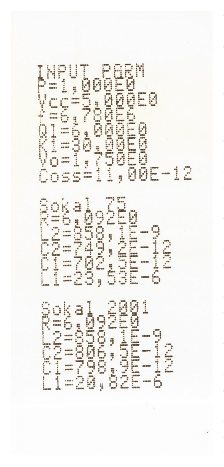
In order to stop working at the PC for so long, I started using the calculator more often to find optimum parameters and just do a short simulation at the PC. Here's the print out from the calculator.

QL is the Qload of the circuit, K1 is the ratio of XL1 to XC1 (unadjusted) (mentioned in Sokal 2001), one could do some iterative calculations but a simple adjustment seems good enough.
Simulations, unfortunately are not handled (yet) by my HP42S... so here's the ngspice output.
Spice output using 2N7000 Vgs=5V

There was something wrong! After having a closer look at the datasheet of the 2N7000, the drive voltage was clearly a problem. My system is 5V only (Vcc and Vdrive) and it is clearly insufficient to fully drive the 2N7000. Once the drive was changed to 12V the waveforms looked much better.
2N7000 with VGS=12V

Since the system will be 5V only I had to find a logic level drive MOSFET, the ones I had available were IRLD024 or IRLR024N. Unfortunately there are no spice model available for the IRLD024 (Vishay or IR), so I will use the second one (IRLR024N) for simulation and the first one for the final circuit.
Class E with IRLR024N
This last waveform starts showing some signs of out of tune (VDS is 5V at turn-on) but the Sokal documents give hints on how to tune.

2013-02-26

Class E deambulations

I've been recently been "pointed the way" to change/learn new engineering skills and (with some reluctance at first) I decided to embrace RF (as in radio frequency) as the way to go.
As any semi-nerd-academic I started by buying the books, I bought the ARRL Handbook, the then I read a blog referencing to EMRFD. I must admit that RF always sounded difficult, complicated and away of normal engineering. Like a cult or a secret society. No information was ever revealed.... Finding a book having "Experimental" on the title caught my attention and showed me it was probably not the reality.

By the way, I have no plans to become a HAM, I just want to try and learn RF. Because of that I have to use the ISM bands available (and within reasonable power less than 2W, radiated probably less than 0.1W).

I'm still reading (in the engineering way) both books, but after some reading I decided it was time to build something.

Having worked in power electronics (and in the light of my new "interest") I decided to build something I knew was used both in RF and induction heating, a class E amplifier/driver but I had no personal experience.
Class E was defined by the N. and A. Sokal in 1975 with a US patent 3'919'656
(Nov 11, 1975) and in 2001 new refined design equations were presented in QEX Jan/Feb 2001 (also by N. Sokal).

My requirements are simple to start with output power 1W, a 5V supply, a Vswsat 1V, operating frequency 6.78MHz (ISM band and I also have a Short Wave receiver that receives this frequency), Qload 6. This is all you need, if you use the 2001 formulas determining L1 will be iterative (the 1975 formulas should be OK and are not iterative).

Having seen a few pages (here, here and here) using the 2N7000 and having tons of them, I decided to use it in the project.
Being a bit academic I calculated the values, substituted the NMOS with a voltage controlled switch and simulated the circuit.

Schematic for simulation of a Class E Amp
The results were very encouraging...
Voltage and Current in the Class E Amp

In the picture above v(500) is the switch voltage, v500#branch is the switch current and the v(900) (sinusoid) is the load voltage. The power in the switch was also relatively low with an average below 1W (V500 is a 1V source to simulate a voltage drop in the switch). This without tuning the circuit (but also without a real 2N7000). 
Power through the Switch
At this stage, I saw enough to go to the second step, simulate with a "real" 2N7000, but that's another story.

2012-10-21

It works! Opentherm Interface V2

We're Back after a very long break!

Last January I presented a schematic for a second version of Alex's JeeTherm to Opentherm interface.


Well Alex finally had the time to test it and it works.... almost :-)
The first part of the board related to the physical interface actually works (!) i.e. sending and receiving the bits and packets to the boiler. This part was done with good old technology and using an operational amplifier as an active load.


The second part of the board was designed to power the remote controller from the loop power supply. This one we knew it would be trickier.
Placing the small supercap (0.1F) as load of the regulator was a good idea as the regulator is output short circuit protected so charging current is maintained within reasonable levels. Our fear was that due to the big charge current for some time on power up, the boiler would give up communicating (part of Opentherm interface, in case a boiler is connected to a plain old thermostat).
The key problem was that the display, the backlight (even when disabled) and the Jeenode take too much current for the system to be reliably powered...
We will have to arrange a winter sunday meet to fully debug these problems...

2012-02-26

FireFly Jam Jar (2)

After a mostly uneventful February, except for the smell of winter we had with week below -5C and snow (2 hours, but just enough to spread havoc in the Dutch transport system), I finally decided to post something.
My FireFly hardware is finished, including the bricolage of painting the glass. I mixed a part of pebeo vitrea 160 frosted medium with yellow colour of the same line. The LEDs are in yellow and orange so a similar colour to enhance the effect seemed appropriate. I used a sponge to enhance the frosted glass, I didn't want Luísa to see the electronics inside (it kind loses the magic). This is how it looks after baking.


On the top I placed one of my solarbotics SCC3733, I opened two holes in the top and fixed the solar panel with two part epoxy glue, I then scraped the epoxy until I found the contacts and connected the board.


It doesn't really look that good, the photo is over exposed and you can't really see the mess I've made... not only the two components were not thoroughly mixed, there are lots of air bubbles in the resin.

Finally I also glued the board to the top of the jar.


You can just see the drill under the board and the wire connecting the solar panel to the battery charger. The jumper powers just the circuit but leaves the battery charger charging.

Now it is just software, the current code is running from the Reindeer Christmas Ball so battery runs out... fast...
I just checked my first post on this project was here, 5 months ago... I'm very slow... very very slow...
The idea of having it with the solar panel is to teach Luísa that the "FireFlies" need to be fed (i.e. put on the sun)... the solar panel is also a way to turn it on/off.

2012-01-28

OpenTherm v2 First Prototype

I finaly built a prototype of the opentherm interface (version 2) for Alex to test, since he dosen't have all the tools to test it I'm hoping that at least the physical interface works, the other features are powered through the interface and using a supercapacitor to hold the power during radio transmission.


The board has a JeeNode interface so Alex doesn't have to change much, there are two extra jumpers, one connects the opentherm rectified voltage to the PWR input of the jeenode, and the other connects the 3.3V output of the jeenode to a supercap. It is still a bit oversized but... Well it is a prototype... The OpAmp is the LM358 (dual version of the quad LM324), works from 3V to 33V and it is relatively low power. The specification of Opentherm states a open voltage of 40V so I had to protect the OpAmp with a parallel Zener (seen in the picture).


A lot has to be done on the jeenode side, but it is mostly software regarding the power saving modes and saving enough power before the short bursts of radio transmission. The schematics of this circuit is based on the published before, but I'll hold the final one until Alex gives me feedback.

2012-01-16

OpenTherm Interface V2

As I mentioned when the boards arrived, I'm planning a new board/circuit but I just briefly mentioned it.
Alex pointed out that in the OpenTherm specification it is stated that a master unit, i.e. your thermostat in the living room or a controller (in Alex's case), could be powered by the interface (use google to find the specification).

In the OpenTherm specification the boiler is slave (although providing the current loop) and the master is the remote control unit. He asked me if it could be done, and looking at the first schematic I drafted a battle plan:
  1. get rid of the dissipative receiver resistor;
  2. get rid of the dissipative transmission resistor;
  3. get rid of the optocouplers, (isolation is good and desired but CTR isn't very good for cheap opto's... hence more current).
  4. with whatever power is available, use a LDO and power something.
  5. Design a current loop transmitter (4-17mA)for testing that works at 40V.
  6. Design a two level shunt regulator for transmitting from master to slave.
  7. Design a minimal loss current loop receiver with output to 3.3V logic systems.
The mains issues were, the maximum loop voltage of 40V and the low voltage LDO and digital signals (3.3V)... and size since Alex want's a "shield" for his JeeNode. There aren't many IC's that work at 40V...

I have planed a tribute post to Jim Williams and Bob Pease playing around analog computers, but time hasn't allowed it... so this short one goes to them and to Bob Widlar.

First I had to design the current loop transmitter to test the system, the input had to be 40V so that under lower load the output voltage was close to that (part of the OpenTherm specification). I remembered the LM10 (designed by Widlar) had an interesting feature in it's datasheet, it is the only OpAmp I know that has been specified for shunt operation (Dear TI that page says "all national products now are belong to us" in front of the datasheet is .... lame).
It also had a application schematic for a current controller, I modified that schematic to allow a push-button (4-20mA) switch (for those not able to find the LM10 check here for an alternative way to generate the current loop, replace DAC with voltage generator).


Then was the master transmitter, basically a shunt regulator with two levels, inactive 7V and active 15V. I used two diodes in series as the reference to the minimum voltage for the regulator, there's a hell of thermal drift but I don't expect the temperature to move outside the range 16C-40C with a corresponding error of 120mV and respective change of about 600mV, therefore negligible. Also I added the push-button to change from one state to the other. I thought of using the same LM10 but unfortunately the LM10 is too slow even for the 2kHz output waveform (it is 1kHz manchester encoded), so the next big thing in single supply opamps capable of 30V operation is the quad LM324, I've used the double LM358. They have their problems in precision and audio circuits but they're good enough and fast enough for the job.

Finally I designed the receiver, the current loop receiver was a nice exercise. I used a simple linear converter to adapt the current levels at the current sense resistor to voltages of less than 0,7V (4-9mA) for the low level and greater than 2,0V for the high level (20mA). One interesting point one is that even single supply amps can work with negative voltages as long as the output is within specification and the voltage at the pin is not negative.


And that's it, I just need to wire a small pref board and send it to be tested.

2012-01-12

New Boards arrived!

This time is the PCB of the Opentherm Interface (v1.0) for Alex and his JeeNode and my Jam Jar Firefly simulator.


The round ones are the JamJarFirely and the rectangular is the JeeNode interface. We've sent them to be produced by Lean, there were some delays but eventually we got them.

Alex mentioned that the Opentherm interface mentions having a loop powered Master and Alex wanted to try and do it with JeeNode. I thought about a version two.
I think that I have the hardware ready but surely a lot has to be done in the jeenode side in terms of software, there are only about 25mW available permanently (about 5V@5mA).
This is my first attempt, I've still just tested it on the breadboard but I think it will work. Here is my initial schematic, the LED on the input is a receive indicator and correct polarity indicator (lights dimly when correctly connected and blinks when receiving).


The rest of the circuit is a programmable shunt regulator with two voltages (the transmitter 7V and 16V since the loop is a current source) and a current to voltage converter (receiver).

2011-11-11

TI Launchpad

Recently I've been trying to do battery powered devices and I came to the conclusion that there is more to it than you first think.
My experience with the Bird-O-Matic is that it each battery lasted only 25% of what I had planed. There were some options that might have influenced it:
  • I didn't made an OFF timer, once the PIR detects an warm object it turns ON the MP3 player and the Amplifier for some time (7-10 seconds), placing a forced OFF timer of 20-30 seconds would prevent constant re-triggering every time someone passes by.
  • Was the use of a CMOS 555 better than a micro-controller? Today's controllers consume almost nothing in standby or power down mode, and a wake up on pin changed could be used with the PIR.
  • The external MP3 player consumes a lot of power and takes 1-2 seconds to start up. It was the simpler and fastest solution, but not the best for power saving.
Recently I read about the MSP430 ultra low power capabilities and I wanted to try them out. The Texas Instruments Lauchpad let's you do just that at a very low price (about 10EUR) and a big Windows installation (see here). I admit I'm always very reluctant to install windows software but unfortunately these links for installing in Linux didn't work out.


It is a bit sad, but I'm no sysadmin and no I don't know perl and I don't want to lose time learning perl, to correct a script, to install a msp430-gcc, to program devices... I understand the technical difficulties behind maintaining and supplying a gcc distribution (specially if also sell a payed tool), but nowadays it is becoming a "must". Sounds like when AMD started giving away PALASM... suddenly every PLD manufacturer started doing it or... went out of business..
After installing the correct tool (the free version is not the latest version), I followed the start up guide and sure enough I made my first C program.
The tool is simple and powerful (based on eclipse), in Windows everything works mostly out of the box.


The board is "divided" into a emulation tool and the experimenter board where devices of 14 and 16pins can be connected. There's also the option of soldering (an included) SMD low-power crystal oscillator. Instructions are also provided on how to measure the power of the experimenter processor, although it is tempting do not cut the board through the dashed lines.. it will not work as a MSP-ISP... that's another tool. (but I guess removing the jumpers and direct connection is ok :-).
The processor although a 16bit simple RISC architecture does appear to be quite capable, I just tried out a couple of examples in C. This though is not what I want to try out... I want to see if the operating current is as low as "advertised", but that will have to be for a another post.

Christmas Ball (the 11.11.11 post)

It is a bit late to announce but we won a prize!!!


Huyser bookstore in Delft ran a competition to promote the book from Arne and Carlos "55 Christmas Balls to Knit", see the promotional video here. Just before the deadline (1.11.11) our son Daniel was born, but we managed to find time to finish the Ball and submit it.
Naturally Ana chose a pattern and knitted the ball, I took care of the electronics. We were so late entering the competition that we only have "night shots" before submitting the ball...


It is a simple ATTiny15L powered with 3x AAA alkaline batteries.
There are 4 LEDs connected to the ATTiny, each in one of the reindeer's nose.
I've made a 32bit pseudo random number generator with a LFSR. The ball to lit is randomly picked (1..4) and also the fade-in time (1-2sec), fade-out time (1-2 sec) and off-time (2..4 x 2.5sec i.e. number of watchdog cycles).
The average measured power consumption is 1.5mA so one can expect about 1000 hours of operation from 3 standard cells.
(click on the circuit for a better view)


The schematic is not exactly this one, this is for another project that hopefully will come out before Christmas, just remove the solar charger, the voltage measuring and that's it!
We got the third prize, 100EUR in books!!!

2011-09-28

FireFly Jam Jar

I wanted to build a night-lamp for Luísa, something a bit less "spooky" than a blue IKEA Spöka that she has. I also wanted to be able to charge just by placing it in the sun (even there isn't much of that up here)...
I went back to my stack of old ATTiny15L and designed a circuit with four LEDs connected in a particular way that only used 3 pins to lit each of them. The other two measure external light (light on when it is dark) and battery (low bat... do nothing be very very still).
I got some jam jars and some Yellow/Amber LEDs and started programming, for the battery I selected a 3.6V 50mAh NiCad (i.e. junk hanging around) and the battery charger was a two transistor current limiter but after some tries I settled with a simple schottky diode from the panel to the battery.


The idea of the project is that when night falls (or lights out) the light goes on for about an hour hopping from one light to the other with different ratios of fade-in and fade-out. This hopefully will induce a sleepy feeling (like candles... by the way.. simulating four candles is also possible)
The schematic is the same as for the reindeer ball project, but this time I went "all the way" to a PCB FAB. I still have to wait for it to come but it looks nice in the preview.


It is my first "non-rectangular" board and actually my first milled board. We'll see how this project will look like in the end...

Alex OpenTherm interface for JeeNode


Alex requested a "quick and dirty prototype" for his Opentherm JeeNode interface. He has more details on the "substance" here and here. I just made the boards, it is all his design (boards plural, the first one was wrongly mirrored, b.t.w. it is the wrong one you see on the pictures).
I followed the usual toner transfer method, and just works, HEMA photo paper is the best! The second board is not so pretty.... but at least it is correct (no photos of this one though).
The schematics are on Alex's site but here's my second try at the schematics also:


Here a detail of the board where you can see some "over etching":

Bird-O-Matic

Pedro asked me, some time ago, to do a collaboration project with a good friend of his.
The idea for the installation art project was the story "The Nightingale" from H.C. Andersen, the idea was to build/make a talking bird of sorts. Our initial plans had to change somewhat substantially... here's what we did:


My part, was to design and build the electronics that would "make the bird sing", we already had the bird's voice in a mp3 track (a danish Nightingale!!), we just needed something to play it. The original idea was to have a bird (just like in the story), but one of the places was an open air installation, so a bird cage seemed a better option.

The first constrain was time, we had only two months for doing the first "bird-o-matic". We gathered a PIR Sensor, a MP3 Player, and a LM386 amplifier IC from Solarbotics.
We wanted a reasonable sound volume so we chose a 9V battery to power the circuit, this is challenge because these batteries do not have a big capacity (max about 1000mAh) and we still wanted to play for some time without replacing the battery. This also excluded from the start using an Arduino as they consume a lot of current even if you manage to put it in standby.
I decided to use a simple monostable (LMC555) triggered by the PIR sensor that would activate the MP3 player and amplifier for a reasonable time (enough to play the nightingale sound). I used low-power MOSFETs for the power switching and one as inverter.
The first build used a LM78L05 but these have a very high quiescent current (~4mA), 10x more than the PIR sensor alone(~350uA)! The second choice was the LM2950 with only 40uA without load (increases to about the double with load) The LMC555 also has a lower quiescent current when operated at 5V (100uA) when compared to 9V (~160uA), and orders of magnitude lower than his "high power" counterpart the LM555.
Still the total current in standby was lower that 600uA, this would give 2000 hours in standby!
Playing... well "you can't make an omelet without breaking some eggs", the MP3 player consumed about 80mA and the LM386 another 80mA, giving a total play time of about 6 hours, still quite good if you think that the track was only 20 seconds... that is about 1100 times... it also exceeds the LM2950 maximum current by 50% but it works until it is too hot then the thermal shutdown "kills the bird" (battery saving on the cheap).
Here is the schematic:

Here is a close up of the inside of the bird cage:

Here a photo of the first prototype:

2011-03-05

Tot Ziens Stuut en Bruin

Last 26th of February one of the most iconic Electronics shops in the Hague closed its doors after 63 years... Stuut en Bruin you'll be missed. After two months open in 2011 (and some nice IC sales), they finally gave in to modern trends and closed the shop.


The picture above was take on the last Saturday, where the sign "there's still 1 day" was on the window.

Here is the google.maps picture

View Larger Map
We are now left with two other shops that are more focused towards other fields (satelite and consumer electronics and electronic/electric spares).
It is sad... but life goes on...

2010-12-31

New Year's resolutions...

This year is coming to an end and this will be my last post (this year). I didn't post as many times as I wanted (I planned once a week, I'm close to once every two weeks), but that's the way life goes.
Most projects are "work in progress", so these are in plan for next year:
  1. in the mini68k I wanted to finish a working gdb-stub before advancing to the CP/M-68K code. I finally managed to make it work, but there were some bumps in the way. The way ahead is not without it's perils, to use gdb and CP/M at the same time I might need an extra serial port for which I have no breadboard space. I'll need to draw the schematics, possibly make a PCB, make the SDCard interface work and then port CP/M to it;
  2. in the mini85 I wandered off in some hardware questions (casing, with a floppy or without, processor speed, with DMA, cheap DMA, video, expansion, connectors, front panel, size of RAM, SD Card, SD Card removable, Flash or Eprom, serial ports, parallel port...). I'll need to settle down on the hardware, draw schematics, make PCB, fit in a case and close it;
  3. in the Solarlight project I still want to fit it neatly on top of my Pepper pot and to tune some more code, also add a larger heatsink for the LED. I also plan to do a new SMD PCB and bake the components in a SMD oven. Further, I'd like to build a bike light with the same circuit but no solar charger. I'll need to get the final schematic, draw the SMD PCB for solarlight and bikelight and make the code linux-buildable and downloadable;
  4. in the SBC6120 project I'll need to decide on how to fit everything inside the box and fix the harddisk to the PCB, also design the front panel, back panel and connectors.
  5. in the home monitoring project I'll need to rewrite the code for the new light sensor and adjust the pachube data to it.
I don't think I'll run out of electronics projects for next year, but if just in case I do, I have to change a pedal crank on my Kronan (got bent on a recent fall on the snow) and I'm waiting for some studded tires :-) , read some more books and try to reduce a bit the coffee intake...

2010-10-28

SMD help

I sometimes boast about my old SMD soldering skills to my "happy hacking" friends... It's quite safe, until someone actually asks you to do _this_! Alex bought some of these JeeNodes from JeeLabs and needed some help. I accepted the challenge...
Before we start, a word of wisdom... Don't try this at home if you don't have the right tools, if you are uncertain about your tools or your ability it is best to send the module to JeeLabs and he'll repair it for you.
Following the site it is easy to understand the problem, Vout and Vin are connected to the wrong sources (this is a linear regulator Vout must be lower than Vin). The solution appears easy but it was not clear from the pictures, once the IC is in the vertical, there are two sides to chose from.
I usually start with the board to repair over a clean sheet of paper, makes easier to see as there's a better contrast, also if some small components come off the board or need to go in they're easy to see.
I then apply a small blob of solder to each side of the IC. The blob keeps liquid for some time and allows you to heat the other side (it must be a quick movement), once both sides have liquid solder slide the IC off the PCB to the paper.
Then using solder-wick clean the excess solder on the pads and on the IC feet.
I then marked the pads and the IC feet with the numbers and visualized what I had to do.
The IC actually is placed in "dead bug" style (but sideways), this means that the IC is "top-to-bottom", it is not so clear in the JeeLabs pictures.The mechanical pencil is 0.3mm for reference.
Finally I used some wire-wrap wire to connect the "floating-pad" to the board.
Since I have no idea how to connected to the JeeNode, connected it to the USB port and checked if the output voltage was around 3V... Some LEDs blinked (like in Arduino's FTDI), no smoke or hot ICs, I suppose it's fine...
SMD reputation intact...hopefully :-)
PS. - google.reader.friends if you have two posts one with pictures and other without pictures, it's just me and my faulty brain...

2010-07-06

Prototype PCBs with Toner Transfer

I wanted to redo my old Munny project and build a new versatile PCB that had a minimum ATTiny15L system with in circuit programming (ICP). I planned the RGB LED and the temperature sensor to be soldered on the edge of the board, like having solder tags. The rest would be the CPU, the programming connector and the minimum number of components (a few resistors and a capacitor).
Although I've already managed to use gEDA to design and send a PCB for fabrication, I wanted to try going "DIY" and have a faster "turn around" from project to board. The board would also be very small (about 2cm²) the cost of making a production run wouldn't be cost effective.
Before I've used the UV light transfer with very good results, even for double sided boards. This time I wanted something even more "barebones" only the etchant, no other chemicals (like the extra developer in UV photographic method). I found some sites with the reference to Toner Transfer Method. They used either inkjet glossy photo paper, a specific "Press and Peel" paper ending in common "glossy magazine" paper, there's even a nice page at Make: web discussion . I decided to give it a try!
First I designed the board single side only. I started out with 10mils/10mils/0.8mm (10/10 means 10 mils tracks and 10 mils minimum spacing between copper, a 10 mils is 0.01 inch; the last number is a minimum drill), but soon I had problems connecting the ICP with the defined tolerances. I changed to 6/6/0.8mm and finally managed to connect everything and pass the DRC test. The next step is printing.


My printer is a HP laserjet 4L (its old, 300dpi but it works!), it still has some problems that I didn't quite worked out yet. There is some rendering on the edges of the lines that I didn't managed to "clear out", I think it is the REt setting but I didn't managed to disable it with my linux driver (the printer is network connected), this is something I would like to solve. It might be visually more appealing when printing normal graphics, but for this particular purpose it doesn't work! Here's a picture of the zoomed output.
As you can see the horizontal lines (in the photo above, to the printer they're vertical lines) and edges have a "saw tooth" on both edges. As I said before I think it is a rendering/dithering that the printer "self" does to make the lines more eye appealing or it is a misaligned mirror.
I tried out 3 different types of glossy inkjet photo paper from Dutch shops. Bellow the three different papers ready for cutting and ironing to the board.


I obtained the best toner transfer with the HEMA glossy photo paper, not bad for the cheapest of all the options...

The transfer was clear and sharp... all the rendering artifacts appear in the copper. The paper that doesn't show has peeled off easy, the part that is attached is the one you have to scrape.


The first from the left actually when it transferred to the copper the toner transferred fully but in some areas it got stuck to the paper. It might mean that this paper need more ironing time, temperature or pressure (or all of the above)... I might try it again... the one in the far right is the HEMA paper, needs more scraping but the toner sticks to the copper fully.


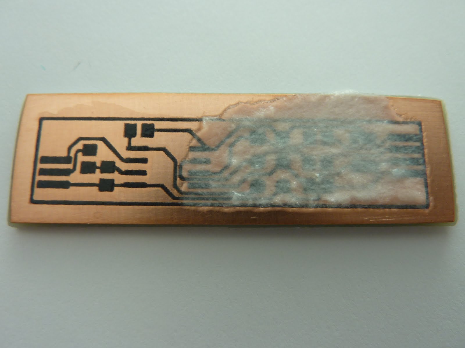
This is the view of the most troublesome area, two wires going between two pins of the ICP and one track between pads of a SMD resistor, both around 6/7 mils clearance. I had to puncture the centre of the pins because I forgot to set "drill" in the print out and it helps a lot for drill bit centring.
I actually had to separate the track from the SMD left pad, the etchant didn't go through the little spot of paper (visible on the picture above). The picture bellow I removed the toner and performed an electrical test with the multimeter. I also drilled the connector.

After that stage I soldered the components and had my board running after a couple of minutes. Here's the final result. The power connectors below the board have been soldered for testing and programming, I'll be removing these... I'm also planning some tests and improvements to the board's software.
The connector ICP is a 6 pin female because it has a smaller (in height) footprint than the male connector. I'm quite please with the LM35CZ and RGB LED footprints, for such a small projects edge placement is viable and saves board area.
Getting the 6/8 mils was a bit of an over achievement and it is only viable because the board is small and hasn't got many connections, 10/10 mils should be the standard. I also need to see if I can solve the rendering of the printer problem... maybe (God forbid :-) using a Windows driver?
The soldering was done by hand and normal soldering iron, a "next step" would be an SMD-oven.
Tah Dah!