Showing posts with label gEDA. Show all posts

2013-03-24

HF on the ATtiny15

I wanted my class E amplifier to be driven by an Attiny15. The idea is to build a HF (6.78MHz) low voltage and low power beacon.
The maximum PWM frequency attainable using the factory OSCCAL value, and using OCR1B=2 and OCR1A=1 is 8.525MHz with the only possible duty cycle is 33%. With OCR1B=3 we get 6.393MHz, OCR1B=4 we get 5.115MHz.

I want to use my beacons in the ISM band of 6.78MHz so the second value (OCR1B=3) is the closest. I managed to output a duty cycle of 25% (OCR1A=1) or 50% (OCR1A=2), this is perfect for a class E drive as 50% is available. The final tuning was done with trial and error on the OSCCAL value until I got the correct frequency.
In my tests, the factory value for OSCCAL (of all the Atmel Tiny15L I tested) would get you within 1% of the nominal frequency 1.6MHz, but with frequency measurement and tuning I got to within 0.5%.

Did a couple of other idiot measures and observations.
- The program memory of the ATtiny loops, the PC is only 9bits and when the last instruction of Program memory is reached execution continues for 0000.
- A NOP consumes less current that an rjmp +0, not significantly but noticeable. I fill the memory with each instruction and measure the current with or without BOD. The second instruction also take double the time of execution.

RJMP+0,BOD - 3537uA (AVG)
RJMP+0,NO BOD - 3494uA
NOP,BOD - 3503uA
NOP, NO BOD - 3458uA

- OSCCAL after reset is cleared and the measured clock frequency is 1.1MHz, when taken to 0xFF the frequency is 2.083MHz.
- Clock jitter of the oscillator. I filled the program memory with the following:
lp000:
.rep64
sbi portb,portb1
cbi portb,portb1
.endr
rjmp lp0000

I would then trigger the scope at the low level at the end of the loop. This gap would last longer than normal, then it is easy to trigger on it. You can just see it under the trigger arrow in the picture above.


I would the trigger to the flank increase persistence to max and let measure. the jitter.


The waveform goes up quite fast (in less than 10ns) with the oscilloscope probe as load. With a gate of MOSFET... it's not so good...

2013-03-02

Class E - selecting a switch

After the initial results (with a simulated ideal switch) here, had to design a real circuit. Having seen a lot of projects with the 2N7000 and having a few in my surplus bin, I used it in the simulation.
Finding spice models for the 2N7000 is easy, being the only problem that there are so many. I used the typical Coss of 2N7000 (11pf) and subtracted from C1 in the Sokal 2001 formulas.
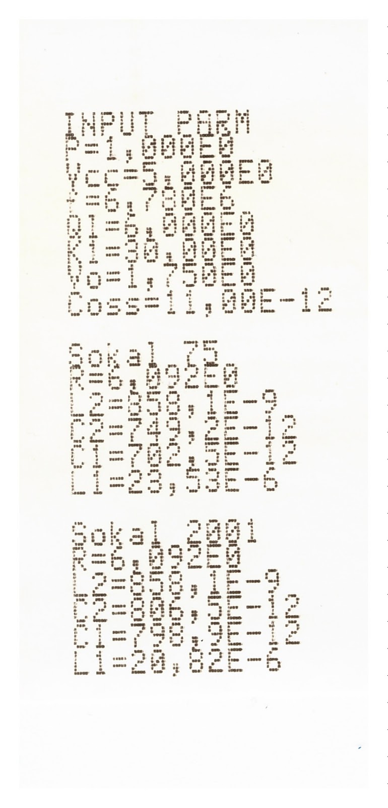
In order to stop working at the PC for so long, I started using the calculator more often to find optimum parameters and just do a short simulation at the PC. Here's the print out from the calculator.

QL is the Qload of the circuit, K1 is the ratio of XL1 to XC1 (unadjusted) (mentioned in Sokal 2001), one could do some iterative calculations but a simple adjustment seems good enough.
Simulations, unfortunately are not handled (yet) by my HP42S... so here's the ngspice output.
Spice output using 2N7000 Vgs=5V

There was something wrong! After having a closer look at the datasheet of the 2N7000, the drive voltage was clearly a problem. My system is 5V only (Vcc and Vdrive) and it is clearly insufficient to fully drive the 2N7000. Once the drive was changed to 12V the waveforms looked much better.
2N7000 with VGS=12V

Since the system will be 5V only I had to find a logic level drive MOSFET, the ones I had available were IRLD024 or IRLR024N. Unfortunately there are no spice model available for the IRLD024 (Vishay or IR), so I will use the second one (IRLR024N) for simulation and the first one for the final circuit.
Class E with IRLR024N
This last waveform starts showing some signs of out of tune (VDS is 5V at turn-on) but the Sokal documents give hints on how to tune.

2013-02-26

Class E deambulations

I've been recently been "pointed the way" to change/learn new engineering skills and (with some reluctance at first) I decided to embrace RF (as in radio frequency) as the way to go.
As any semi-nerd-academic I started by buying the books, I bought the ARRL Handbook, the then I read a blog referencing to EMRFD. I must admit that RF always sounded difficult, complicated and away of normal engineering. Like a cult or a secret society. No information was ever revealed.... Finding a book having "Experimental" on the title caught my attention and showed me it was probably not the reality.

By the way, I have no plans to become a HAM, I just want to try and learn RF. Because of that I have to use the ISM bands available (and within reasonable power less than 2W, radiated probably less than 0.1W).

I'm still reading (in the engineering way) both books, but after some reading I decided it was time to build something.

Having worked in power electronics (and in the light of my new "interest") I decided to build something I knew was used both in RF and induction heating, a class E amplifier/driver but I had no personal experience.
Class E was defined by the N. and A. Sokal in 1975 with a US patent 3'919'656
(Nov 11, 1975) and in 2001 new refined design equations were presented in QEX Jan/Feb 2001 (also by N. Sokal).

My requirements are simple to start with output power 1W, a 5V supply, a Vswsat 1V, operating frequency 6.78MHz (ISM band and I also have a Short Wave receiver that receives this frequency), Qload 6. This is all you need, if you use the 2001 formulas determining L1 will be iterative (the 1975 formulas should be OK and are not iterative).

Having seen a few pages (here, here and here) using the 2N7000 and having tons of them, I decided to use it in the project.
Being a bit academic I calculated the values, substituted the NMOS with a voltage controlled switch and simulated the circuit.

Schematic for simulation of a Class E Amp
The results were very encouraging...
Voltage and Current in the Class E Amp

In the picture above v(500) is the switch voltage, v500#branch is the switch current and the v(900) (sinusoid) is the load voltage. The power in the switch was also relatively low with an average below 1W (V500 is a 1V source to simulate a voltage drop in the switch). This without tuning the circuit (but also without a real 2N7000). 
Power through the Switch
At this stage, I saw enough to go to the second step, simulate with a "real" 2N7000, but that's another story.

2012-02-27

Mini85v2

And now for something completely different, not only do I take an enormous amount of time to do something, I also overrun myself with different projects...

After a year or so of designing PCBs and sending them for fabrication, I finally decided to go for the big one and design a full Eurocard (160x100mm) computer. I have enough confidence on my EDA package (gEDA) and myself to design it, and the prices are also relatively low for a double sided board so I'm jumping to it.

When I dismantled the breadboard mini85 I promised to do a PCB version (this was in 2008!), so here I am back on it 4 years and 2 kids later!
The idea is about the same, build a minimally usable CP/M system on a eurocard, with standard TTL logic circuits, minimum I/O, a switching power supply for the computer and the drive, which is a 3.5inch floppy on top using the high density (1.44Mb).


I've been scaling down from the initial idea of having 512k of SRAM and a paging arrangement and a 8256AH as a UART and parallel port (like my 68k project... that, by the way, is also on hold...), and slowly going back to the simple original Mini85.

I even had a port for system configuration and dip switches, but this version (below) no longer has a MMU.

I think that I am finally setting for a 8085 at 8Mhz connected to a upd765 and a software UART with SID, SOD and RST5.5 lines, memory will probably be 64K SRAM (w/ 32K paged in/out) and a 32k ROM. An ON/OFF switch, a RESET, a TRAP and a RST7.5 interrupt push switches.

2011-04-09

SBC6120 - Power Supply Board

It had been planed for ages, but I never had the time or a technical "consideration" delayed me. I finally decided to just do it (after reading the "cult of done" manifesto), the board with the Laser Toner Transfer and HEMA inkjet photopaper, this was probably the biggest board and with the least detail I've ever done (160x120mm).

The board needed only to fix the connectors, the power switch and a switching power supply. I didn't have much space available on the top side, so I went through my "pile of components" and found a couple of single IC switching power supplies (the National LM2575-5V), I also had a SMD version of it (or so I thought) and some SMD Schottky diodes. The board is also used to mechanically fix the 3.5 inch Harddrive.


The schematic was simple, just the switch, the connectors and the switcher, I added a turn on delay to let everything power up slowly (see the LM2575 datasheet).


The power switch (and the lever) are from C&K, but I had to buy an "old lever" as the new levers are much wider than what I could "afford" in terms of space on the front panel (there's no bezel for this older one though).
For the PCB I had some problems, but mostly mechanical. You can only see them when I show the pictures of the completed unit. I had to fit a 10mm inductor in a 10mm space and a 3.5 inch harddrive in 3.5inch (minus 1mm space, there's a screw on the harddrive I had to remove, otherwise the top would not close.

This is probably the only reason why I'll do boards at home, it must be a big board (>160mmx100mm), few tracks and single side, if it misses one of the tests, I'll go for a Fab. board.
After assembly... it didn't work... A quick trouble shooting revealed the cause... poor eyesight.
I had a LM2595S not the original LM2795 with which I drew the schematic and PCB. The pinout is very different. Then I found out I had no LM2975 SMD version. I had to improvise, a through hole package with bent leads and plenty of flux later...


After that mishap, I mounted everything back up and it worked. I formatted the drive and downloaded a disk image and now my SBC6120 boots!


It was done in two weeks! I'll try to keep this "cult of done" thing going on (but some of the tasks need to be broken in more than a couple of weekends).

2010-11-13

Hardware Single Step for the 8085

As usual my current developments tend to wander towards all directions, as the ever expanding universe... Although I haven't really finished any of my other "side jobs", I want to further develop the mini85 into a real single board CP/M computer, but more on that later.
This week, I looked for a Hardware Single Stepping circuit for the 8085. Something that proves that "everything is on the internet" is not true (if you didn't already knew), at least until up to now.
The internet came up with nothing, so I had to resort to older methods... Books, applications notes, etc... First of it was the 8080 datasheet, on the description of the READY line it states "Can be used for single stepping the processor" but this sentence is strangely absent from the 8085 datasheet (a nice circuit with one wait state is drawn instead). Then I found something on a great book "Microcomputers and Microprocessors - The 8080, 8085 and Z-80 Programming, Interfacing, and Troubleshooting" by John Uffenbeck. There are caveats, about the same as others and my previous pseudo-DMA circuit for the 8085, doesn't allow the use of dynamic RAM hidden-refresh (end of M1). I've redrawn it with gschem.


It is not exactly what I want. I want a single lever switch with 3 positions RUN, HALT, SingleStep. I found this one on Digikey a nice C&K switch that "has the looks" of a 1980 Computer and could do the job. The problem is that I need to do some adaptation from the schematics above to a single switch with 3 positions, the main problem is halt the computer when the switch is off (centre position) and at the same time set the FF clock low... I might need some magic...

2010-02-27

SolarLight (7) - Software, AVR assembly


Ok, finally google docs supports any type of file so I can post all the project files in one place: code, gerbers, gEDA design files and spreadsheet with the calculations, requirements. It is all here.
I decided to try out pastebin, so I'm updating this post with the code for everyone to take a peek... In this version I'm still working on the "when to turn on" routine, I think it still doesn't work as I initially intended... pastbin doesn't look so good to paste long assembly lines, but here it goes anyway..

The software as it is now is working, it has some problems and "room for improvement" but it is working! You know the motto: Make it work, make it better!, make it faster!

One of the improvements would be to limit the time the light is ON to about 30min-45minutes, this would allow the battery charge to progressively increase during the good sunlight days and progressively decrease on a sequence of bad sunlight days (as in this year for example).
Other improvement could be a full darkness detection and adjust a 12h no light clock from there. It has happened that during the day when a big cloud (and/or heavy rain/heavy snow) the measured light level goes down to the "night" level, then if there's enough battery the light turns on... it shouldn't and I'm sure this winter is exceptional, but the only way to prevent this is to detect the lowest darkness point and count 12 hours from there, and only from then on the light would turn on when it is dark.

In the code I added a debug routine that is included when the two variables are uncommented (DEBUG and DB_CNT), when I wanted to output a value I load it in the DEBUG variable and call dbug. The byte is output in the status LED serially MSB first, there is a long (2 cycles) high pulse followed by clock and MSB data, clock and bit 6 data... clock and LSB data.

Finally my biggest problem was the branch instructions, the AVR has the following:
BRLO - Branch if Lower (UNSIGNED)
BRLT - Branch if Less than (SIGNED)
BRGE - Branch if Greater or Equal (SIGNED)
BRSH - Branch if Same or Higher (UNSIGNED)
I was not used to have these complex branch instructions, I'm used to Zero Flag set, Zero Flag Clear, Carry set, Carry clear... I'm specially not used to having a different branch for signed or unsigned... So I chose wrong.. result the jumps were not taken when they should. The ADC values are unsigned when read (0..255) but if you start calculating with them you can get signed (negative) values and then you have to use signed instructions.
AVR assembly programmer beware!

A final word about the Code, it was assembled with Atmel AVR Studio Assembler (Win), it doesn't output the number of cycles per instruction... a bit of a let down... :-)
And with this post I finish this project.... Woo Hoo!! Project is dead, long live the new Project...

SolarLight (6) - PCB Fabrication and Assembly

Using gEDA for producing gerbers turned out to be easier than I thought.
Recently the gEDA project has been under fire in slashdot due to its "complicated", "non intuitive interface" and lack of documentation. I really don't think that the documentation is that bad, it is scattered but it is not bad, just look here. I haven't meet an Open Source project that didn't suffer from the same problem, even (and particularly) the GNU tools. As soon as you get out of the mainstream gcc/gas/ld/gdb you're almost on your own, searching bits and pieces in the internet. Some of the best GNU project documents have been written by a commercial enterprise (either redhat, cygnus or other).
I call it Anarchic-Knowledge (or Anarco-Conhecimento in Portuguese), everyone omits to write what he finds trivial, forgetting that what is trivial to him, might not be for the community that will use the product. Then a plurality of tutorials, blog posts and guides show up, each one showing how they did it "their way". A new user has to pick all these pieces, try more than one and finally write a "I did it my way" post... And we all learn from this experience.It is not the lack of documentation, it is just the way that Open Source grows.
Back to the how I did it... :-)
I followed this tutorial, I had a single page schematic so it was easy to generate the netlist. I created a single project file with the schematic libraries, I used my own symbols since not only I wanted to learn how to do them but also I had a MOSFET with two Drain Pins that I could use each in an independent circuit. I used shell scripts to get the job done, I tried once a Makefile but I realized that I would have to change the Makefile for every project (even smaller ones), a shell script can do that at invocation time.
I also created some Footprints for my project (also for educational purposes), I had them in a library directory and used jcl's gnetlist invocation but with my directory instead. PCB must also be configured to have a pointer to your library in the "File-Preferences-Library".
First follow what gschem2pcb tells you to do, open the file, import the parts, spread them and execute the command, then I put in most of the mechanical details, using the outline layer in a place where no components were place, size of the board, cuts, groves and fixing holes. Also check now for the DRC tolerances in the File-Preferences Menu.
Then the fun begins, it is a very iterative process: place, route, looks good? can I do it better? with less vias? other mechanical problems? heat sinks/problems? repeat until satisfied with the design.
Then I place some more information on the silkscreen, plus signs on the connectors, output indication, board reference, moved the references so that all are visible when the components are soldered and facing the same side (so that you don't need to rotate the board to read the references). I also place on the top and bottom layer a square with the layer number inside, so that you can identify the layers on the gerbers and on the boards.
I was going to use Olimex pcb prototype services for my first gEDA boards so I needed to limit the number of drill sizes, they have some drill sizes that are considered standard and any other is considered extra (and you pay more), luckily someone from the gEDA-user group already made a drill mapping file for Olimex after executing the script run DRC again! Here's my final PCB result.
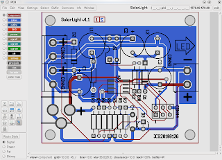
You can also export to png the two sides of the board in a "photo-like" picture, some people claim it gives better reading and it is easier to spot errors.

If you have no errors in the last DRC you're ready to produce your gerbers, and this part is as easy as pressing the correct button in export. Then with gerbv, check if the gerbers look nice and the drill sizes are correct.
Recently a good question came up in the geda-user mailing list, it sums it up nicely but the first reply reminded me of something I didn't do and should have done...
Print out your surface copper layers and put the parts on the printout to make sure they match.

yup, I designed my resistors with a 1/8W in mind and then I couldn't find any I had to use 1/4W.. so the resistors didn't fit in place. My DIP 4 for the MOSFET also didn't had big enough holes, apparently International Rectifier didn't stick to the normal DIP drill sizes, probably due to current capability or thermal conductivity. In that point, with some hindsight, I would increase the copper area connected to the drain, that could be a good heat sink for the MOSFET. I also should have thought a bit more on how to fix the board to the pole, with the new batteries the SolarLight is much heavier, I should have devised other way to fix it. Here's the board in place, note the resistors in two layers.
UPDATE: The resistor that is hanging and has two sockets is the gate resistor of the MOSFET, if you check the spreadsheet with the calculations you can see that the gate current has great influence in the MOSFET power (losses), so I made it low enough to still allow programming easily (now at 100R). When programming the micro the light turns on, but without any damaging effect as long as the frequency (of programming is high enough 250k) and the pattern is sufficiently random (see here for a bigger problem with ISP port sharing).


One last remark, if you buy microcontrollers in ebay and they say "New, Old Stock" it doesn't mean that they are not programmed, they can be factory programmed and that doesn't mean that they are not new! In case of the ATTiny15L, the low voltage programming mode can be disabled by this factory programming, if you solder it to the board you'll not be able to reprogram it. You need to remove it from the board and use a HVProgrammer like AVRDragon for example. Learned the hard way...

2010-02-17

SolarLight (5) - PCBs!!!

I finally had the time to pick my PCBs at the mail. I was thrilled to see who it went... My first linux made PCBs!
Everything went ok, except for a few minor point where I'm the only one to blame...
Here are the pics to the solarlight board and the others, the last one is the RFadaptor that didn't go as well as I expected, but I'm the only one to blame....
Here is the one where the wholes are just the size of the pins (just not enough for them to get through)...

I'll post how to get from PCB design to send them to Olimex (for example) for production. It's not that difficult but you need to follow some steps.

2010-01-30

Thinkpad X40 and openSUSE 11.2

Note to self... and anyone interested... Installing openSUSE 11.2 in a IBM thinkpad X40:
- edit partitions yourself (don't trust a computer to do a man's job), create primary partition, don't format as ext4 use ext3 instead(see update notes below), mount root; create primary partition, format as swap - size must be at least half the memory (just used for hibernating);
- install the languages you want (for OpenOffice dictionaries);
- disable firewall (avoids frustration when playing with toys);
- install development in C and KDE;
- remove Games (although some bastards are hard to kill);
- remove AppArmor, Beagle (optional, but if I don't know what they do, I don' t want them);
- install minicom (to play with serial toys);
- install kate (resonable window editor);
- install zip and other utils;
let it install for an good hour...
let it auto-update... let it fail...reboot...
let it auto-update again... now everything looks green... (the SUSE updater icon);
search for "opensuse 11.2 restricted formats", don't read any warnings and go directly to the one-click install... click yes, accept import keys and "deny any wrong doing" regarding the dvd-read library.
When finished reboot and have some food/coffee. Your system is ready to work... but for curious minds continue....
Search "opensuse 11.2 science" click on opensuse_11.2 and copy the URL, open YAST and add a repository using the URL that you cutted, add and import key...
In YAST go to software management and search for the following:
- gEDA (install all programs);pcb (install pcb); gerbv; ngspice, gspiceui, gwave2;
- AVR (install binutils,gcc, libc, avrdude);
Search "OpenOffice updates stable", install repository as above.
Open Yast and then Software Management, select All in "package groups", in the programs window select "all in this list -> update if newer version is available"
That's it, your laptop is a electronics design workstation and avr cross development computer.
Some things of opensuse need some extra work like SUSPEND and HIBERNATE, I also didn't managed to get dual head working "out of the box" and I'm reluctant to change the Xorg.conf... something I did when I had my first thinkpad a second-hand 340...

And all this because I had a Sony reader for a week and then decided to return it (takes to long to render some PDFs with pictures, and sometimes it hangs), wanting to un-install calibre... I found out there is no such thing... damn!
Update: my old backup software failed first to copy the ext4 partition and then failed to install grub for booting. After battling with it for some time I decided to do a fresh install with ext3. It is a pain in the butt! I hate myself for it, I should have known better, you should never be an early adopter!

SolarLight (4) - gEDA, PCB and first corrections

It has been a while since my last post, but I've been busy... not so much on electronics projects, but projects of other kind... Nevertheless I've been working a bit on SolarLight.
The prototype was working to light the LED but some other bits of the code were not working. Although the "light-on" function was working, the function checking the battery and checking the charging were not.
After wake-up from reset (power-up or watchdog), the micro checks if the current Solar Panel voltage is >200mV than the battery (a safe assumption it is charging) and if so increments a "charging timer", if this timer is less than 3hours, don't turn the light on. This is to be sure that there is some charging before a discharge. These and other checks were not working.
De-evolution from C to Assembler is always a mess if you have to re-learn the mechanics of each architecture. It is not only the instructions, its how the micro "thinks", only then you really control the machine.
On the hardware side I also had some problems, due to the limited number of pins I had to share some pins with the in circuit programmer, one of them is the MOSFET gate. I forgot to add a gate resistor to the source, in common MOSFETs with 10V gate threshold that is still asking for trouble, I guess that with LL (logic level) gate thresholds of 2V it is just "waiting to happen"... although it did take a couple of weeks...
I guess what hapened was, after programming the AVR-ISP left the pin floating and probably before that the level was high... the MOSFET kept on and finally burned.. I saw smoke coming out...
Here the new schematic with revisions on the lower corner.I also started the PCB design (with PCB part of gEDA suite) and I've now finished the board. It is not as packed as it could be because it has the size of a 3xAA pack. It is marked version 1.1 because I had finished the version 1.0 when the MOSFET blew up. I've mostly followed the tutorials available at the gEDA Documentation site:
- this one for the drawing of schematic and creating the netlist;
- this one for drawing footprints and getting to know PCB;
- and this one for the simulation;
- I also used this one for creating large "box symbols" (cpu, uart, etc)
I used gschem directly to create the new MOSFET symbol (IRLD024), since the original MOSFET symbol was graphic I though it would be better to use it instead of having a 4 pin box. I also wanted to keep both Drain connections separated if needed to use them in separate nets (although they are connected).
Using gEDA is still far from trivial as components, footprints, schematics symbols are all your responsibility, but still, I'm starting to like it. PCB also has a nice feature, you can print "photo mode" version of your PCB (yes, I know other software produces 3D views), here's mine top side.

2009-11-27

SolarLight (2) and gEDA simulation

An update over SolarLight, I finally managed to print waveforms from ngspice in OpenSuse 11.2 . For some reason the interface is not what you would expect and it has become much more complicated to print a waveform than before.
The first time I installed gEDA from the sources (under OpenSuse 10.3), now I'm using a precompiled version from the OpenSuse Science repository, it could be that the precompiled version has the printer interface "disabled" in some way.
Back to waveform printing, under ngspice one would follow the following path to simulate and plot a waveform:
tran 100n 1.5m
plot v(501),v1000#branch

In the case of the SEPIC circuit of a previous post this would run transient simulation until t=1.5ms with a minimum time step of 100ns (try not to have more than a few thousand simulation points), the second line would open a new window with the output voltage and LED current displayed.
Previously when I pressed in the hardcopy button the print interface would appear and I could chose the printer and/or print to file. Now a message appears in the console:
The file "/tmp/hc4803" may be printed with the Unix "plot" command,or by using the '-g' flag to the Unix lpr command.

If you try the "lpr -g" command either the system complains that it is not supported or that no printer is installed.
lpr: Warning - 'g' format modifier not supported - output may not be correct!
lpr: Error - no default destination available.

After installing plotutils I managed to convert the plotted file (hc4803) to almost any known format (for example postscript or png) with the command:
plot --output-format ps hc4803 > hc4803.ps
plot --output-format png hc4803 > hc4803.png

This allows the plots to be printed and included in documents or webpages, the plot looks something like this:

Then I wanted to try out gwave, gwave is a waveform viewer, part of the gEDA package but its use is far from trivial. First in gwave you must run a simulation and then write the data to a file:

tran 100ns 1.5ms
write plotdata.dta

then run gwave with this data.

gwave plotdata.dta

The interface is far from trivial, I was unable to use colours for the plot and I also had error while trying to print a plot, but at least I could see some waveforms. Results may vary depending on your installed system, but here is a screenshot of the program, the waveforms are in gray on black background:


I'm now temped in building the gEDA toolsuite from scratch... but for that I need some more time...

2009-03-29

Munny Hardware

A viewer asked to see the schematic and the BoM of the Munny project and finally had the time to do it. I didn't managed to produce a good schematic print, but I'm learning... I'll try to improve it...

The part list is the following:
U1 ATTiny15L (this part is obsolete)
U2 LM35CZ
U3 RGB LED from Sparkfun
R1,R4 10K
R2,R3,R5 100R
C1 10uF 15V
C2,C3 .1uF

I'll try to automate better the parts list with gEDA I'll post it again (using gnetlist ...something) and then I'll try to edit it to include datasheets and link to supplier.
As soon as I manage to assemble the program in linux with avr-gcc (avr-as) or have a C program compiled for the Attiny15 I'll post the software.

2009-01-10

gEDA, Spice and small circuit simulation

In my "quest" for a suitable Electronic Design Automation set of tools in Linux, I wanted to test the ngspice in gEDA. I started by reading this tutorial.
I designed a simple single transistor amplifier and draw the basic circuit in gschem. The circuit is a commonly called fixed bias circuit with emitter resistor, for transistor I used a general purpose BC548B.
For drawing the schematic one should use the symbols in the spice library and draw the circuit as usual with the following cares:
- you must remember to place a ground in one of the nodes.
- if you want you can (and should) give numbers to nodes you want to keep track, this is done by editing the netname of node, later it is easy to find and plot the voltages of each node.
- it is better to create a separate file with the models of the semiconductors you use, to use it in gschem edit the model attribute and add a file attribute with the library path and name. I found out that using a big library of models and using only one model is not efficient and prone to errors, and most of the libraries need some adjustment regarding the model parameters. It is better to create a specific library file in the current directory (like models.lib) with only the models needed for the simulation.

For converting the schematic into a spice netlist, one must resort to some trickery. I created the following bash script to create it for me, it does a design rule check and then converts the schematic to a spice netlist, then immediately runs ngspice.
#!/bin/bash
gnetlist -g drc2 $1.sch -o $1.drc
gnetlist -g spice-sdb $1.sch -o $1.net
ngspice $1.net
My bash scripting talent isn't great, but it should give an idea of what you need to do. This script expects one argument, the schematic file name without the extension (.sch).
Once in ngspice you can run the circuit interactively with :
tran 10u 10m
plot v(1),v(103)
I didn't found out how to save a plot, so I used a screen snapshot and cut the edges of the picture in GIMP, but here is the final result.

There is some delay and some distortion in one part of the wave and the gain is quite small. The base appears to saturate during the high side and then appears to take its time coming out of saturation. The delay is introduced by the decoupling capacitors (input and output) and the voltage gain is limited by the Rc/Re to 5, but then further divided by Rc parallel with RL, for a total voltage gain of about 2.5.
The charging of the decoupling capacitors is responsible for the apparent lack of gain in the first half wave.

2008-12-07

Creating a PCB with gEDA

I always wanted to try out the gEDA tools for producing PCBs and schematics in the Linux environment.
The ongoing mini85 (8085) project is to big for a first try, there are many packages that are not standard in gEDA, many schematic symbols that also do not come standard, there are many ICs in the schematic, these are too many variables to control for a first time.
I needed something smaller, where I could fully test the tools. I decided to use my USBHID Flight simulator control for this project. I would also try out other things like adding a MACH131SP because it is a SMD component, programmable via a ISP connector (also test the software) and test the package outline of a DB9 connector, the power connector and USB B connector.
I want to send the board for fabrication, most of the PCB fabrication houses need a gerber file (none accepts pcb format), but not many details appear in the official tutorial.

The schematic editor has a reasonable sized library, but if a symbol is needed the procedure is quite fast, I used tragesym and the tutorial is here. I redesigned the symbol for the Atmel AVR AT90S2313 (also ATtiny2313), because I prefer to have direct access to the VCC and GND pins and I don't like the crystal oscillator and the reset input in the bottom. Here is the first page of the schematic.


For converting to PCB I downloaded a library from jluciani, it seems very complete... I still have to understand how to use it properly and in conjunction standard libraries. It needs a small modification of the command line of gsch2pcb.
gsch2pcb --use-files --elements-dir ~/footprints SCHEMATIC_NAME


For now I think the footprints provided are suficient, but I'll probably need to draw new footprints for some older PGA microprocessors (when the time comes)...
Another way will be to try the same system with kicad, it also appears to be a good (free) design tool for linux. It has an extra that for now I don't really need which is the 3D view, but who knows latter...