Showing posts with label 8085. Show all posts

2012-02-27

Mini85v2

And now for something completely different, not only do I take an enormous amount of time to do something, I also overrun myself with different projects...

After a year or so of designing PCBs and sending them for fabrication, I finally decided to go for the big one and design a full Eurocard (160x100mm) computer. I have enough confidence on my EDA package (gEDA) and myself to design it, and the prices are also relatively low for a double sided board so I'm jumping to it.

When I dismantled the breadboard mini85 I promised to do a PCB version (this was in 2008!), so here I am back on it 4 years and 2 kids later!
The idea is about the same, build a minimally usable CP/M system on a eurocard, with standard TTL logic circuits, minimum I/O, a switching power supply for the computer and the drive, which is a 3.5inch floppy on top using the high density (1.44Mb).


I've been scaling down from the initial idea of having 512k of SRAM and a paging arrangement and a 8256AH as a UART and parallel port (like my 68k project... that, by the way, is also on hold...), and slowly going back to the simple original Mini85.

I even had a port for system configuration and dip switches, but this version (below) no longer has a MMU.

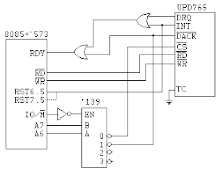
I think that I am finally setting for a 8085 at 8Mhz connected to a upd765 and a software UART with SID, SOD and RST5.5 lines, memory will probably be 64K SRAM (w/ 32K paged in/out) and a 32k ROM. An ON/OFF switch, a RESET, a TRAP and a RST7.5 interrupt push switches.

2010-11-13

Hardware Single Step for the 8085

As usual my current developments tend to wander towards all directions, as the ever expanding universe... Although I haven't really finished any of my other "side jobs", I want to further develop the mini85 into a real single board CP/M computer, but more on that later.
This week, I looked for a Hardware Single Stepping circuit for the 8085. Something that proves that "everything is on the internet" is not true (if you didn't already knew), at least until up to now.
The internet came up with nothing, so I had to resort to older methods... Books, applications notes, etc... First of it was the 8080 datasheet, on the description of the READY line it states "Can be used for single stepping the processor" but this sentence is strangely absent from the 8085 datasheet (a nice circuit with one wait state is drawn instead). Then I found something on a great book "Microcomputers and Microprocessors - The 8080, 8085 and Z-80 Programming, Interfacing, and Troubleshooting" by John Uffenbeck. There are caveats, about the same as others and my previous pseudo-DMA circuit for the 8085, doesn't allow the use of dynamic RAM hidden-refresh (end of M1). I've redrawn it with gschem.


It is not exactly what I want. I want a single lever switch with 3 positions RUN, HALT, SingleStep. I found this one on Digikey a nice C&K switch that "has the looks" of a 1980 Computer and could do the job. The problem is that I need to do some adaptation from the schematics above to a single switch with 3 positions, the main problem is halt the computer when the switch is off (centre position) and at the same time set the FF clock low... I might need some magic...

2009-06-02

My DRAM circuit works!

Well, after some tests I'm confident that my 8085 DRAM interface is working properly!
My first test executed from EPROM and at the end of every instruction fetch cycle does a CAS-before-RAS (C-B-R) refresh.
The second test wrote a value to the DRAM and latter read it back, still executing from EPROM, a C-B-R refresh was done at every instruction fetch.
The third test I tried writing once and read many times, and if at some point the values differed halt the processor (this would terminate refreshing). It worked, no Halts!
On the fourth test I decided to go a bit more ambitious, not only I initialized the stack to the DRAM I also placed a RET instruction in the DRAM. The program in the EPROM would then call the RET instruction and return to EPROM. This would trigger an instruction fetch in the DRAM and respective hidden refresh.
Here's a picture of the execution of the RET instruction and respective hidden refresh, top signal is RAS bottom is CAS.


Done, my "home-made"dynamic ram refresh circuit works, now I'll have to try with other microprocessors...

2009-05-24

8085 DRAM interface (30 pin SIMM)

After seeing this project on Make (or here) I felt like old DRAMs could have a better use... It is a bit sad that so much technology and development by semiconductor engineers and computer designers goes "wasted" on a light box. The light box looks good, don't get me wrong.. but.. so much engineering wasted in a light box... doesn't look right.
I always thought that using these SIMMs in microprocessor applications would be interesting and with the proper memory management it could be used with old 8 bit microprocessors. The likes of Z80, 8085, 6809, 6502 could go with a simple DRAM interface.
Trying to search for information online or even in books, application notes etc is quite elusive, there are three good sources of information:

  • This one (or here in pdf) is very specific regarding the Z80, and Z180...[...]

  • This one with a PIC processor connected directly to a DRAM chip (source code only).

  • And this one, where a FPGA and a 8051 microcontroller are connected to a 72 pin SIMM.

  • Most of the microprocessor or microcontroller projects online either use one or more large SRAMs (128K,256K and 512K bytes) are these are nowadays readily available.

    Although my projects don't need a large RAM size I wanted to probe the use of old SIMMs with the 8085. The Z80 makes it all a bit more simpler because it has been design to use DRAMs, so at the end of the instruction fetch cycle the RFSH and MREQ signals go low, the problem with this that the instruction fetch cycle is slightly (half cycle) shorter (see here).

    It seems logical the one would try to do the same in a different processor, while the processor is decoding and executing the fetched instruction the DRAM controller preforms a DRAM refresh, this way every instruction fetch a refresh is performed which normally is often enough. Except, in the 8085 case, if the processor is halted. The Z80 solved this problem by still performing instruction fetches during HALT (it executes NOPs). I decided to carry on accepting this problem and do not write any programs that halt to processor unless I want to lose the contents of the DRAM.

    In the 8085 there's no refresh cycle, but at the end of every instruction fetch, during 1 to 3 cycles (depending on the instruction just fetched), the CPU relinquishes the bus, these are called T4,T5 and T6 states (see here). Although a single cycle for refresh might not seem a lot, one could extend the cycle a bit more until ALE goes high, from then on the address on the bus is valid and a normal fetch should be made.

    The 8085 does have an slight advantage when compared to the Z80 (and Z8000), the read signal and write signal (RD and WR) are active for the same time weather in instruction fetch, memory read and or memory write (and even I/O these are extended in the Z80), so there's no need for a early-write signal when using the SIMMs.

    I designed the circuit as a combination of two sequential circuits, one generating RAS, CAS and Address inputs during a normal read/write and instruction fetch (accessing), and another circuit for refreshing the RAM on every instruction fetch (refreshing). During a instruction fetch from a non-selected memory the last cycle is used to do a CAS before RAS refresh, if the fetch is done from the DRAM, the access cycle is extended to do a hidden refresh (toggle of RAS line while CAS is low). When ALE goes high all DRAM access activities stop and the circuit waits for RD or WR to go low to start the RAS/Address Mux/ CAS sequence. I use the X2 output from the 8085 because it is at 2 times the CLK output, therefore it allows faster state switching and a longer memory access time.


    I've designed and assembled the circuit and I'm about to do extensive testing if it really works or not. Here's the schematic of the CAS/RAS generation, the connection to the SIMM is straight forward, the pin-out of a 30-pin SIMM is here, and some of the history of SIMM development is here.


    The 8085 is clocked at 8MHz, and on the oscilloscope RAS appears on top and CAS on the bottom. My only problem has been my EPROM emulator, and I need to do something about that in the future. It is only working in DOS... So now I need to do all the programming in DOS and test the system with the oscilloscope. I'm also using the SOD line to trigger the oscilloscope when the SIM instruction is executed, the current program is the following (beware, 8085 assembly follows):

    .title test_program 0
    .sbttl testing

    .area ram(abs,cseg)

    .org 0x0000
    reset:
    di
    lxi h,0xC000
    lp000:
    mvi a,#0xC0
    sim
    mov a,m
    jmp lp001
    lp001:
    mvi a,#0x40
    sim
    mov m,a
    jmp lp000

    2008-12-22

    Mini85 has left the building...

    I decided to dismantle the Mini85 circuit to gain some desktop area for the next year. It was the biggest and more complex breadboard project I've ever done. I did not manage to build it in three standard breadboards, but I still find it small enough. With a single PAL (maybe a 16V8) I'm pretty sure it could fit the three boards.
    The next step is use what I've learned from this Mini85 project add it to the PCB design and USBKeyboard and build a eurocard (100x160mm) CP/M computer.
    Here is his last picture in this format...Mini85 "will be back" soon... in PCB format...

    2008-11-02

    Formating a floppy in Mini85

    My list of softwear and hardware tasks is becomming shorter by the day. That is the number of new tasks added during the week is less than the tasks I finish during the weekend...
    This weekend I finished the formating function and the display help function. On the hardware I changed the regulated power supply by a home build switching power supply, I've also changed the Motor on timer to 30 seconds to reduce wear on the floppies.
    I've also created a task lisk on the blog's front page so it's easy to keep track of the TO DO list on the Mini85. I think it is a good idea, to keep a todo list for each project while it is running.I'll keep a list alive and maintained until a new project comes along, then I'll do a new one.
    The format routine had a few details, the interrupt routine had to be changed to support the read/write operations and format operations.

    Two pictures of the switching power supply, pretty standard. An LM2575-5.0 simple switcher, a RENCO 330uH inductor with IRMS 3 Amp capability (an old sample I had) and a schottky diode 1N5819 (here the diode is only capable of IRMS 1A)...


    2008-10-18

    Using a CP/M Simulator

    Since I started the project I started searching for CP/M simulators. In order to boot and use my system I needed a tool to build CP/M (assembling the CCP,BDOS,CBIOS and CBOOT), and transfering files to the disks. I found many that are a bit outdated here, and two great simulators with loads of cp/m software ready to run: Z80pack and SIMH/Altairz80 .

    I setteld with Altair Z80 SIMH because it suited better my project. On the processor side allows you to change form the standard Z80 of most simulators to a 8080 processor, you can easily reduce the memory to 32Kb, it also has the boot disks and source (although in Z80 format) for CP/M 2.2, CP/M 3, and MP/M II. Finally and also very important, not only it supports the disk format I wanted to use (3.5 inch 1.44Mb, i.e. as used by P112) as also supports accessing the floppy disk directly.

    As recommended here, I used a image file to transfer the files and then used NTRAWRITE to transfer the files to the floppy. I am using a USB 3.5 inch drive and the other usual tools to read and write CP/M disks didn't work as they used direct access to the UPD765 in regular PC.
    The procedure is easy, start altairz80 and type in:
    sim> set hdsk1 format=p112
    sim> attach hdsk1 \\.\B:
    sim> show hdsk1
    HDSK1, 1474KB, attached to \\.\B:, P112, WRTENB, QUIET,
    T:160/N:18/S:512
    sim> go

    At the moment I can only use CP/M 3 for reading and writing the disk images, because for CP/M 2.2 one needs to adapt the bios specifically for each hard disk.
    When all the files have been transferred to the disk image, close the simulator and use NTrawrite to write the floppy image into the floppy.

    2008-09-30

    8085 CP/M computer

    It is amazing how the ideas flow once you put the schematic on paper... or screen... I wrote a list of possible improvements for the next circuit iteration.

    Hardware:
    - try (again) changing the FDC765 clock circuit down to 4MHz;
    - change the FDC interrupt to RST7.5;
    - change CRT_RXD input to RST6.5;
    - change RDR input to RST5.5 (instead of SID);
    - change PUN output to one of the 74HC259;
    - do a system request input in INTR or TRAP inputs;
    - do the LPT interface (with STROBE and PERROR);
    - upgrade the system to full 64k bytes. (play Zork!)
    - decide what to do with SID input and SOD outputs ?
    - lights for RDY, INTA, floppy, etc..
    - add the switching power supply and the MOTOR ON one-shot to the schematics.

    Software:
    - disable CRT/RDR interrupts while on FDC read/write cycle (blocks the system);
    - put the processor in HALT while waiting for a character (save power);
    - implement the RDR and PUN functions;
    - implement the LST function;
    - during a warm boot, read the operating system all at once instead of sector by sector (faster);
    - change interrupts to follow the hardware changes above;
    - either put most of the BIOS in ROM (32K) or in upper RAM (64K).

    The problem with the 64K expansion is that it would use a second RAM IC, that takes up valuable breadboard space (as I have a three breadboard limit), plus probability of failing due to wiring. I think I can still make some more optimizations on the IC's used.

    2008-09-28

    Mini85 - First Circuit Schematics

    The first version of the schematics is finished... There are still some optimizations to do, specially regarding the logic gates. The resistors in the directly connected to the 8085 are not really necessary but handy if a later expansion is needed.
    This part of the circuit also include the FDC-DMA blocking circuit, the IO decoding and the Memory decoding and the reset circuit.


    The second sheet holds the Memory (ROM and RAM), the addressable latch for swapping RAM/ROM and a single Output bit for the serial port (CRT_TXD).


    The third sheet holds the floppy disk interface, data separator FDC9216, write clock divider, Drive interface and floppy connector.


    The forth sheet (still to come) will hold the switching power supply and the motor on circuit.
    It is still difficult to print schematics with gschem, I tried the light output but it is not the best, I'll have to try again with light background and no colors. I will also try to print out a list of connections to do the wire wrapping circuit.

    2008-09-21

    Finished the Hardware

    I had one last hardware modification to try out, changing the clock of the disk system to 4MHz would save some power (due to the reduced clock), spare an inverter (buffer) and reduce the noise interference.
    It turned out it could not be done, at least as far as I tried. The data separator FDC 9216 cannot read 500kbps without an 8MHz input, from the datasheet it is impossible to get that rate without an 8MHz clock. The WRCLK divisor could work but I would need to change the divisor ratio, but the 765 didn't seem to like the 4MHz clock at all as it was unable to read any sector, even increasing the byte loop and changing the specify parameters.
    Finally I have a reached the final hardware configuration for this project. My current IC count is only 16!
    • 8085AH-2 @ 4MHz (8MHz crystal)
    • 74HC573 (address latch)
    • 27C256 (EPROM emulator 32K bytes)
    • 62256ALP-10 (system RAM 32K bytes)
    • MAX232 (serial interface)
    • 7400 (used as 4 inverters...!!)
    • 74HC139 (address and IO decoder)
    • 74LS08 (address decoder, only 2 ports used)
    • 74HC259 (addressable latch, serial port, memory flip)
    • LM555 (motor on delay)
    • 74HC161 (WRCLK divider)
    • UPD765 (Floppy Disc Controller IC)
    • 74HC14 (FDC Interface to the drive)
    • FDC9216 (Data separator for 3.5 HD drive)
    • 74LS32 (FDC Interface to the drive)
    • 74LS240 (FDC Interface to the drive)

    There might be some more optimizing to do, I'm going to try and use gEDA gschem to draw the schematic and I'll post them as soon as their finished.

    2008-09-18

    Mini85 first CP/M boot

    It's alive! There is still a small bug, but I think I've found it already... The Warm Boot sequence (after a CTRL-C) fails. I'm probably not moving correctly the sectors from the disk buffer to the correct place in memory, since the cold boot routine (just after reset) is woring ok.
    Next I need to clear this bug and try some CP/M software that runs in 24k since my system needs 8k for the operating system. Since I am using a "standard" CP/M format of a not-so-old CP/M system (P112), and this format is supported by CP/M 3 running in simulator SIMH (the version emulating the Altair), I can create disks and transfer files from the simulator to the real Mini85.
    Update: I managed to write a Floppy with a copy of CP/M 2.2 startup disk used in SIMH, corrected the warm boot code, and I filmed the boot sequence with some daylight.
    Here's the new video...

    2008-09-07

    Creating a CP/M boot sector

    In Andy Johnson-Laird's book "The Programmer's CP/M Handbook" the major steps of bringing up your own CP/M system are well explained and in this order:

    1. Create your new BIOS with the appropriate device drivers in it. Assemble this so that it will execute at the top of memory (and determine the start address of the OS).
    2. Create the new versions of the CCP and BDOS with all addresses inthe instructions changed so that they will be correctly located in memory just below the new BIOS. (Nowadays you can assemble this code instead of using MOVCPM)
    3. Create or modify a CP/M bootstrap loader that will be loaded by the firmware that executes when you first switch on your computer.
    4. Using Digital Research tools to bring the bootstrap loader, CCP, BDOS, and BIOS in the first tracks of the floppy. (I used my ROM monitor for this).

    I skipped steps 1 and 2 because in a previous "incarnation" of the system I did it and I know it will be the not so dificult part. So I rewrote my Monitor disk read and write to be a little more "efficient" and used them in the bootstrap code.

    After a RESET, the 8085 checks if there is a disk in drive. If so, seeks drive 0 (or A:) to track 0, and tries to read sector 1 (sector zero does not exist, only for historical reasons) into memory address 100H.

    Then jumps to address 100H if it contains the byte value 0F3H, it is the code of a disable interrupts instruction (DI) in the 8080, 8085, z80, nsc800 family of microprocessors.

    The bootstrap loader then reads the rest of operating system into memory (CCP,BDOS,BIOS) from the first track (sectors 2 and on). Then a jump is made to the cold boot function in the BIOS, then CP/M starts.

    I used SIMH and CP/M 2.2 for assembling the code, I fell in a little trap with ASM. It recognizes the instructions SIM and RIM as labels not as instructions... I only found this by reading the assembler print out. I had to use a DB 30H for SIM and a DB 20H for RIM, then it worked ok.

    The Boot Sector Code is posted here.

    2008-09-03

    More pseudo-DMA circuits

    In my search for new alternatives I found two more schematics in a very good article. The article titled "Floppy Disk Data transfer techniques" by T. Marshall and J. Attikiouzel and was published in IEEE Micro in December 1983. The article is a bit Z80 centric but easily adaptable to other microprocessors.

    The first technique is using a edge triggered interrupt and the HALT instruction (NMI in the Z80 or RST7.5 or TRAP in the 8085), the interrupt routine is void but although in the z80 it is automatically cleared on interrupt entry, on the 8085 two extra instructions must be used in the ISR.

    The second technique is the WS (wait state) insertion while waiting for the floppy to get the data. This is a similar technique to the one I'm using in the mini85, the schema proposed has more control options as sensing the interrupt call and determine an error, conditional enabling of WS insertion.

    On the Z80 both these methods allow and profit in terms of timing by executing the INI instruction, one instruction fetch with 3 operations executed (IN (C),INC HL,DCR B).

    Hopefully I will use a combination of both methods, WS insertion for data reads and writes and halting the processor for seek/recall operations.

    2008-08-29

    The 8085, FDC 765 and Pseudo-DMA operation

    My problems with the previous configuration began when my PC USB-Floppy drive stopped formating or recognizing my modified 3.5 DD disk. A problem that occurred frequently and inconveniently solved by removing the disk and inserting it again.
    After reading about lots of complaints about small disk sizes I decided to go the extra mile and implement the said pseudo-dma circuit and routine for 3.5 HD drives. Yes, I had to ask some more questions in the yahoo group, but someone with infinite patience explained me the easy way to do it. Here is the schematic I used for pseudo-dma and the 8085 to read 3.5 HD floppies.


    The operation of this circuit is the following, the read operation is started and a special IN instruction (addresses 2xH) lock the processor in a wait state and asserts DACK. When the byte is ready (this can last a full rotation of the disk) DRQ is asserted unlocking the processor and completing the read.

    There is a problem with this schematic and my program, if an interrupt occurs during a normal read (signaling an error during the read) the processor is unlocked but the first byte read is already the result byte. Beeing RST6.5 level triggered, when the next instruction to the IN is fetched there is no longer a pending interrupt (765 INT line gets deasserted when the first byte of result phase is read) and the system hangs in execution phase.

    One alternative would be to use RST7.5, it is latched by the processor, but on entry in the interrupt routine one should be aware that ACC could contain the first result phase byte. There is a special case where it could not be! As in an error occurs exactly after reading a byte.

    The big issue is that a read or write during execution phase must be completed at 16us nominal (13-11us worst case) and testing if byte is ready or interrupt is pending takes time.

    My next "development" will be polling interrupts for seek and recalibrate operations, as for the execution phase, maybe go back to the NO DMA mode (ND=1) and use HALT as a wait for interrupt instruction, do the test for results phase and read in the byte.

    As for a latter hardware development would be to reduce the 765 clock from 8MHz to 4MHz and use CLKOUT instead of X2 buffered (save a gate).

    2008-08-28

    3.5 inch drives and FDC 765

    Before I started the mini85 project, I started gathering information on the floppy drives and CP/M interface. I came across this page. It made me aware of a few constraints on my project:
    - it would be difficult to find a project with modern day 3.5 inch drives (later I found this one);
    - they would not use MFM at 1MHz bit rate to achieve 1.44Mb densities because it is too fast for the processor (13us) and some sort of DMA would be necessary.
    I was reading comp.os.cpm and a new yahoo group started for people that would want to build their own CP/M computer. My project was going that way so I joined in, draw up some schematics and started writing code and asking questions.
    After initial hardware development and some code, I managed to read and write a 720k floppy on the mini85. To get the best processor speed and least overhead, the 8085 was running at 10.24MHz (2.5% over clocking) and a 8256AH-2 connected to the CLKOUT (@5.12MHz) for the serial interface.
    Regarding the interface between the 8085 and the 765, I used no interrupts (although connected) and polled In/Out as the 8085 is perfectly capable of polling the 765's status and reading the data in less than 26us.
    I was using a PC to read/write/format a normal HD disk with the hole closed with tape, and I was using DEBUG in MSDOS to write sector on the disk.
    As for circuits I tested the one used in prof80 and the one used in the ZX Spectrum +3, in the end I settled for my version of the prof80, i.e. I changed the data separator to a FDC9216 and used a 8MHz clock to the FDC9216 and UPD765, an a 1MHz divider (74LS161) for the 765's WRCLK. I then compromised the 8085 clock to 8MHz so that with a simple change of clock input, either X2 on the 8085 or CLKOUT, I could use 720k or 1.44Mb floppies.

    2008-08-24

    Back from Holidays

    Back from Holidays, a wonderful week in Sardinia with sun, good food and fantastic sea.
    I've tried doing a small schematic with gEDA but in the end I went for "Paintbrush", sorry if my skills are not "excellent". When I use linux I'll try to use Dia or a similar for later postings.

    I've decided to use the SID and SOD lines for auxiliary input (RDR: - reader in CP/M 2.2) and auxiliary output (PUN: - punch in CP/M 2.2).

    I used RST5.5 for direct serial input, the inverter (74LS04) is needed for generating a interrupt (5V) at the start bit (GND), then interrupts are temporarily disabled during reception. A timing loop waits for the middle of the start bit and checks if it is still low (i.e. the RST5.5 pin is at 5V as it is inverted), if not it was a false start bit and exits the interrupt service routine (ISR). From then on reception depends on a software timing loop, inversion of the sensed interrupt line, and shifting the bit in.
    The received character is placed in a buffer and a buffer full flag byte is set. The code is posted below as a picture. I'm still not very "experienced" with blogging and placing code snippets online, so I made a "png" with yellow background, it looked better than any other alternative...

    2008-08-08

    Mini85 - before holidays


    Just before going for a week of holidays in Sardinia I thought it would be interesting to post a picture of Mini85 as it is now. The 3.5 inch drive and the connection to the board. I'm sliming the board as much as I can. I think it is possible to remove one IC or another and/or change one or two of the ICs by one with more or different functions. For now it boots CP/M.
    I'm also trying to develop a AltairZ80 SiMH configuration that resembles the Mini85, I managed to have a 8080 system with 32k of RAM, but then I couldn't build the operating system. I'm also having some issues with the disk format, although I'm using P112 format it only works well in a cp/m 3 configuration.

    2008-08-01

    Back to the mini85

    Today I tried something different on the 8085, and with good results!!
    My first attempt for a software serial port used SID and SOD line for Receive and Transmit signals and bit-bang the serial signals at 2400 baud 8-N-1.
    Then I realized that one of the CP/M BDOS calls needed a different implementation. The functions DirectIO and Read Console Status needed the system to receive a char and keep it in a buffer, until the processor asks for it. Reception must be an asynchronous process!
    I though about it and without changing much of the previous routine, I connected an interrupt line of the 8085 to an inverted receive line. First I tried the edge triggerd RST7.5 detecting the down flank of the start bit (but then using SID line to get the status and then RST6.5 to detect the start-bit and to read the input line. When an interrupt occurred the serial reception routine would receive the character, store it in a buffer and in a auxiliary memory position store a "buffer full" status. The CP/M function could then be correctly executed.
    Instead of using 2 lines (SID and RST7.5), I used only one RST6.5, after the interrupt is received it is possible to "pool" the RST line with the RIM instruction! I save a input line and a few more instructions. It is now apparent to me that the AUX_IN and CONSOLE_IN can both be implemented by software and without using the SID line!
    Removing the 8256 added some other problems, I needed a digital output pin to flip the ROM from 0000H to 8000H (and the RAM the other way), for this I added an addressable latch 74LS259.
    Have a great weekend.

    2008-07-18

    Minimalist CP/M system

    The idea came up last year when I learned that the floppy was considered dead. I decided to go back in time and build the smallest and simplest CP/M computer that still used a floppy (90mm / 3.5 inch) as storage media.
    My project objectives were the following:
    - build a CP/M v2.2 compatible computer;
    - use the smallest number of integrated circuits and the simplest possible configuration;
    - no programmable logic devices, only 74' and 40' series;
    - use a 3.5 inch floppy disk as storage;
    - the console for the CP/M system would be a terminal VT100 (on a Laptop linux/windows);
    - be able to build an fully functioning computer in a breadboard;
    - if possible do most of the software development in linux;
    - build a wire-wrap version of the final hardware;
    - design a PCB, build a box to host it and build a computer.
    I started searching computers I knew that supported CP/M, and based the design from it. I looked at the Amstrad CPC 664 and PCW series, and also at the Sinclair Zx Spectrum +3. All these came from effectively the same place so their floppy disk interface was very similar. The used a NEC UPD 765 and a data separator (FDC 9216 or SED 9240) for the MFM encoding.
    For the processor I settled on a Intel 8085 (8085AH-2) because I had a few in my parts box, it had an on-chip oscillator and seemed simple enough to build the console serial interface with the SID and SOD lines. The extra address decoder 74573 seemed a cheap option compared to the clock generation circuit for the Z80. I also have a NSC800 but not so much hardware information on it. Using the 8085 at 8MHz also allowed me to drive the UPD765 at the same clock or 4MHz with little or no changes. I also had it running it at 10.24MHz, but then the floppy disk needed a separate oscillator.
    For the memory I wanted to use my EPROM emulator bought on ebay and a small enough RAM to run CP/M. I chose a 62256 with 100ns access time and my emulator simulating a 27C256, so 32K RAM and 32K ROM.
    As a help circuit, to get me started with a serial interface and some digital inputs and outputs I added an Intel 8256AH. This IC is not very easy to find but it packs two 8bit ports, a serial interface and some timers. The perfect peripheral IC, a bit like the 6522 VIA for the Motorola 6800 or Rockwell 6502 processors.
    I'll post more on this one.