Using gEDA for producing gerbers turned out to be easier than I thought.
Recently the gEDA project has been under fire in
slashdot due to its "complicated", "non intuitive interface" and lack of documentation. I really don't think that the documentation is that bad, it is scattered but it is not bad, just look
here. I haven't meet an Open Source project that didn't suffer from the same problem, even (and particularly) the GNU tools. As soon as you get out of the mainstream gcc/gas/ld/gdb you're almost on your own, searching bits and pieces in the internet. Some of the best GNU project documents have been written by a commercial enterprise (either redhat, cygnus or other).
I call it Anarchic-Knowledge (or Anarco-Conhecimento in Portuguese), everyone omits to write what he finds trivial, forgetting that what is trivial to him, might not be for the community that will use the product. Then a plurality of tutorials, blog posts and guides show up, each one showing how they did it "their way". A new user
has to pick all these pieces, try more than one and finally write a "I did it my way" post... And we all learn from this experience.It is not the lack of documentation, it is just the way that Open Source grows.
Back to the how I did it... :-)
I followed
this tutorial, I had a single page schematic so it was easy to generate the netlist. I created a single project file with the schematic libraries, I used my own symbols since not only I wanted to learn how to do them but also I had a MOSFET with two Drain Pins that I could use each in an independent circuit. I used shell scripts to get the job done, I tried once a Makefile but I realized that I would have to change the Makefile for every project (even smaller ones), a shell script can do that at invocation time.
I also created some Footprints for my project (also for educational purposes), I had them in a library directory and used
jcl's gnetlist invocation but with my directory instead. PCB must also be configured to have a pointer to your library in the "File-Preferences-Library".
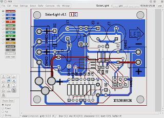
First follow what gschem2pcb tells you to do, open the file, import the parts, spread them and execute the command, then I put in most of the mechanical details, using the outline layer in a place where no components were place, size of the board, cuts, groves and fixing holes. Also check now for the DRC tolerances in the File-Preferences Menu.
Then the fun begins, it is a very iterative process: place, route, looks good? can I do it better? with less vias? other mechanical problems? heat sinks/problems? repeat until satisfied with the design.
Then I place some more information on the silkscreen, plus signs on the connectors, output indication, board reference, moved the references so that all are visible when the components are soldered and facing the same side (so that you don't need to rotate the board to read the references). I also place on the top and bottom layer a square with the layer number inside, so that you can identify the layers on the gerbers and on the boards.
I was going to use
Olimex pcb prototype services for my first gEDA boards so I needed to limit the number of drill sizes, they have some drill sizes that are considered standard and any other is considered extra (and you pay more), luckily someone from the gEDA-user group already made a
drill mapping file for Olimex after executing the script run DRC again! Here's my final PCB result.

You can also export to png the two sides of the board in a "photo-like" picture, some people claim it gives better reading and it is easier to spot errors.

If you have no errors in the last DRC you're ready to produce your gerbers, and this part is as easy as pressing the correct button in export. Then with gerbv, check if the gerbers look nice and the drill sizes are correct.
Recently a
good question came up in the geda-user mailing list, it sums it up nicely but the first reply reminded me of something I didn't do and should have done...
Print out your surface copper layers and put the parts on the printout to make sure they match.
yup, I designed my resistors with a 1/8W in mind and then I couldn't find any I had to use 1/4W.. so the resistors didn't fit in place. My DIP 4 for the MOSFET also didn't had big enough holes, apparently International Rectifier didn't stick to the normal DIP drill sizes, probably due to current capability or thermal conductivity. In that point, with some hindsight, I would increase the copper area connected to the drain, that could be a good heat sink for the MOSFET. I also should have thought a bit more on how to fix the board to the pole, with the new batteries the SolarLight is much heavier, I should have devised other way to fix it. Here's the board in place, note the resistors in two layers.

UPDATE: The resistor that is hanging and has two sockets is the gate resistor of the MOSFET, if you check the spreadsheet with the calculations you can see that the gate current has great influence in the MOSFET power (losses), so I made it low enough to still allow programming easily (now at 100R). When programming the micro the light turns on, but without any damaging effect as long as the frequency (of programming is high enough 250k) and the pattern is sufficiently random (see
here for a bigger problem with ISP port sharing).

One last remark, if you buy microcontrollers in ebay and they say "New, Old Stock" it doesn't mean that they are not programmed, they can be factory programmed and that doesn't mean that they are not new! In case of the ATTiny15L, the low voltage programming mode can be disabled by this factory programming, if you solder it to the board you'll not be able to reprogram it. You need to remove it from the board and use a HVProgrammer like
AVRDragon for example. Learned the hard way...


