2008-08-29

The 8085, FDC 765 and Pseudo-DMA operation

My problems with the previous configuration began when my PC USB-Floppy drive stopped formating or recognizing my modified 3.5 DD disk. A problem that occurred frequently and inconveniently solved by removing the disk and inserting it again.
After reading about lots of complaints about small disk sizes I decided to go the extra mile and implement the said pseudo-dma circuit and routine for 3.5 HD drives. Yes, I had to ask some more questions in the yahoo group, but someone with infinite patience explained me the easy way to do it. Here is the schematic I used for pseudo-dma and the 8085 to read 3.5 HD floppies.
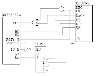

The operation of this circuit is the following, the read operation is started and a special IN instruction (addresses 2xH) lock the processor in a wait state and asserts DACK. When the byte is ready (this can last a full rotation of the disk) DRQ is asserted unlocking the processor and completing the read.

There is a problem with this schematic and my program, if an interrupt occurs during a normal read (signaling an error during the read) the processor is unlocked but the first byte read is already the result byte. Beeing RST6.5 level triggered, when the next instruction to the IN is fetched there is no longer a pending interrupt (765 INT line gets deasserted when the first byte of result phase is read) and the system hangs in execution phase.

One alternative would be to use RST7.5, it is latched by the processor, but on entry in the interrupt routine one should be aware that ACC could contain the first result phase byte. There is a special case where it could not be! As in an error occurs exactly after reading a byte.

The big issue is that a read or write during execution phase must be completed at 16us nominal (13-11us worst case) and testing if byte is ready or interrupt is pending takes time.

My next "development" will be polling interrupts for seek and recalibrate operations, as for the execution phase, maybe go back to the NO DMA mode (ND=1) and use HALT as a wait for interrupt instruction, do the test for results phase and read in the byte.

As for a latter hardware development would be to reduce the 765 clock from 8MHz to 4MHz and use CLKOUT instead of X2 buffered (save a gate).

2008-08-28

3.5 inch drives and FDC 765

Before I started the mini85 project, I started gathering information on the floppy drives and CP/M interface. I came across this page. It made me aware of a few constraints on my project:
- it would be difficult to find a project with modern day 3.5 inch drives (later I found this one);
- they would not use MFM at 1MHz bit rate to achieve 1.44Mb densities because it is too fast for the processor (13us) and some sort of DMA would be necessary.
I was reading comp.os.cpm and a new yahoo group started for people that would want to build their own CP/M computer. My project was going that way so I joined in, draw up some schematics and started writing code and asking questions.
After initial hardware development and some code, I managed to read and write a 720k floppy on the mini85. To get the best processor speed and least overhead, the 8085 was running at 10.24MHz (2.5% over clocking) and a 8256AH-2 connected to the CLKOUT (@5.12MHz) for the serial interface.
Regarding the interface between the 8085 and the 765, I used no interrupts (although connected) and polled In/Out as the 8085 is perfectly capable of polling the 765's status and reading the data in less than 26us.
I was using a PC to read/write/format a normal HD disk with the hole closed with tape, and I was using DEBUG in MSDOS to write sector on the disk.
As for circuits I tested the one used in prof80 and the one used in the ZX Spectrum +3, in the end I settled for my version of the prof80, i.e. I changed the data separator to a FDC9216 and used a 8MHz clock to the FDC9216 and UPD765, an a 1MHz divider (74LS161) for the 765's WRCLK. I then compromised the 8085 clock to 8MHz so that with a simple change of clock input, either X2 on the 8085 or CLKOUT, I could use 720k or 1.44Mb floppies.

2008-08-27

New books and toys!

Today I received my two Arduino Protoshields for some more experiments, a book on home chemistry experiments and other on Fashionable technology. One of the shields is intended to help out a friend with his home automation projects and develop fast breadboard prototypes, the other is for more "fixed" stuff, as a motor controller or a robot interface part.

Here's a photo of the assembled one with a micro breadboard on top and the second PCB (to be assembled).

2008-08-24

Back from Holidays

Back from Holidays, a wonderful week in Sardinia with sun, good food and fantastic sea.
I've tried doing a small schematic with gEDA but in the end I went for "Paintbrush", sorry if my skills are not "excellent". When I use linux I'll try to use Dia or a similar for later postings.

I've decided to use the SID and SOD lines for auxiliary input (RDR: - reader in CP/M 2.2) and auxiliary output (PUN: - punch in CP/M 2.2).

I used RST5.5 for direct serial input, the inverter (74LS04) is needed for generating a interrupt (5V) at the start bit (GND), then interrupts are temporarily disabled during reception. A timing loop waits for the middle of the start bit and checks if it is still low (i.e. the RST5.5 pin is at 5V as it is inverted), if not it was a false start bit and exits the interrupt service routine (ISR). From then on reception depends on a software timing loop, inversion of the sensed interrupt line, and shifting the bit in.
The received character is placed in a buffer and a buffer full flag byte is set. The code is posted below as a picture. I'm still not very "experienced" with blogging and placing code snippets online, so I made a "png" with yellow background, it looked better than any other alternative...