Although I've already managed to use gEDA to design and send a PCB for fabrication, I wanted to try going "DIY" and have a faster "turn around" from project to board. The board would also be very small (about 2cm²) the cost of making a production run wouldn't be cost effective.
Before I've used the UV light transfer with very good results, even for double sided boards. This time I wanted something even more "barebones" only the etchant, no other chemicals (like the extra developer in UV photographic method). I found some sites with the reference to Toner Transfer Method. They used either inkjet glossy photo paper, a specific "Press and Peel" paper ending in common "glossy magazine" paper, there's even a nice page at Make: web discussion . I decided to give it a try!
First I designed the board single side only. I started out with 10mils/10mils/0.8mm (10/10 means 10 mils tracks and 10 mils minimum spacing between copper, a 10 mils is 0.01 inch; the last number is a minimum drill), but soon I had problems connecting the ICP with the defined tolerances. I changed to 6/6/0.8mm and finally managed to connect everything and pass the DRC test. The next step is printing.

My printer is a HP laserjet 4L (its old, 300dpi but it works!), it still has some problems that I didn't quite worked out yet. There is some rendering on the edges of the lines that I didn't managed to "clear out", I think it is the REt setting but I didn't managed to disable it with my linux driver (the printer is network connected), this is something I would like to solve. It might be visually more appealing when printing normal graphics, but for this particular purpose it doesn't work! Here's a picture of the zoomed output.
 As you can see the horizontal lines (in the photo above, to the printer they're vertical lines) and edges have a "saw tooth" on both edges. As I said before I think it is a rendering/dithering that the printer "self" does to make the lines more eye appealing or it is a misaligned mirror.
I tried out 3 different types of glossy inkjet photo paper from Dutch shops. Bellow the three different papers ready for cutting and ironing to the board.

I obtained the best toner transfer with the HEMA glossy photo paper, not bad for the cheapest of all the options...

The transfer was clear and sharp... all the rendering artifacts appear in the copper. The paper that doesn't show has peeled off easy, the part that is attached is the one you have to scrape.
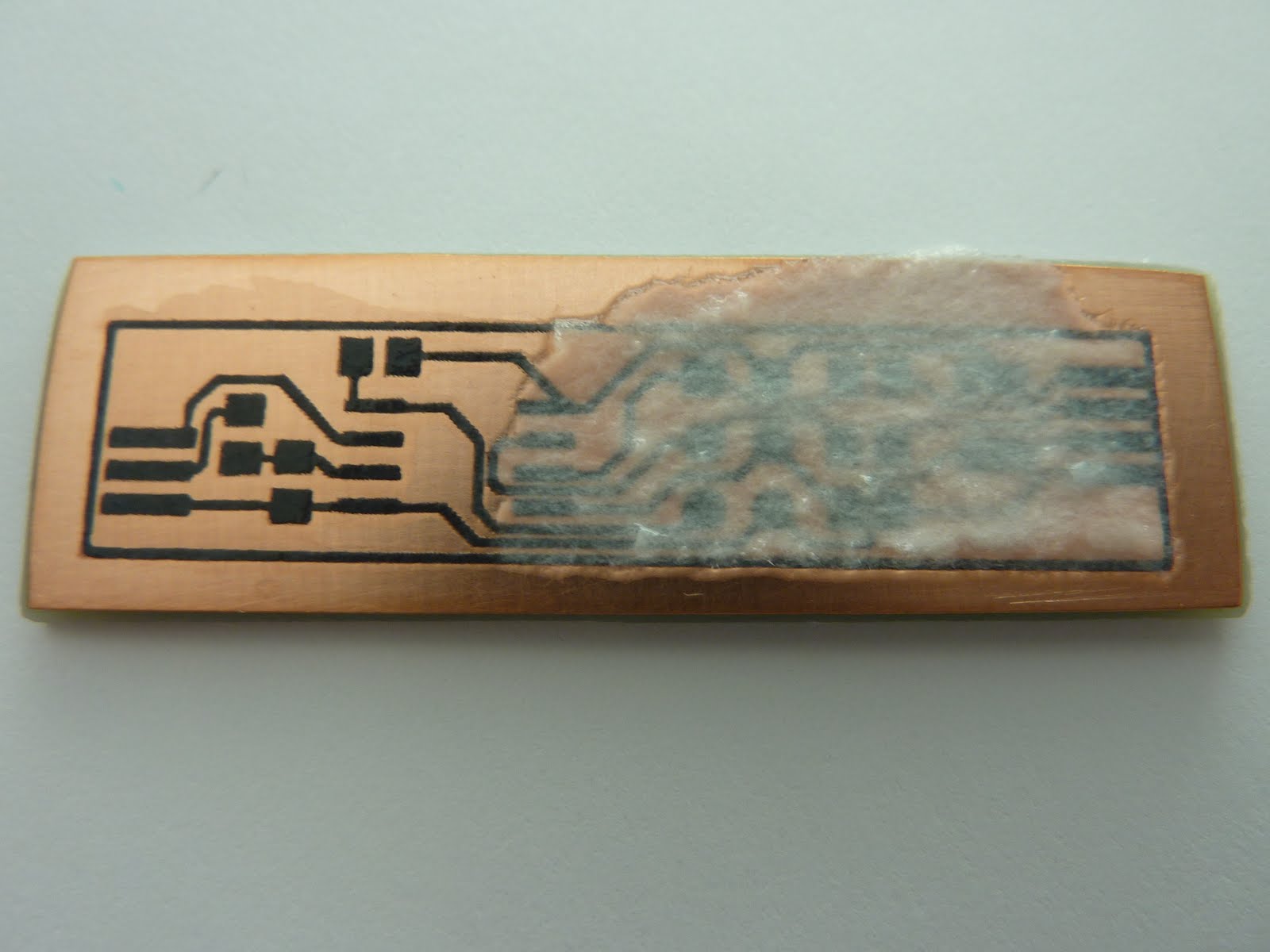
The first from the left actually when it transferred to the copper the toner transferred fully but in some areas it got stuck to the paper. It might mean that this paper need more ironing time, temperature or pressure (or all of the above)... I might try it again... the one in the far right is the HEMA paper, needs more scraping but the toner sticks to the copper fully.

This is the view of the most troublesome area, two wires going between two pins of the ICP and one track between pads of a SMD resistor, both around 6/7 mils clearance. I had to puncture the centre of the pins because I forgot to set "drill" in the print out and it helps a lot for drill bit centring.
 I actually had to separate the track from the SMD left pad, the etchant didn't go through the little spot of paper (visible on the picture above). The picture bellow I removed the toner and performed an electrical test with the multimeter. I also drilled the connector.
 After that stage I soldered the components and had my board running after a couple of minutes. Here's the final result. The power connectors below the board have been soldered for testing and programming, I'll be removing these... I'm also planning some tests and improvements to the board's software.
 The connector ICP is a 6 pin female because it has a smaller (in height) footprint than the male connector. I'm quite please with the LM35CZ and RGB LED footprints, for such a small projects edge placement is viable and saves board area.
Getting the 6/8 mils was a bit of an over achievement and it is only viable because the board is small and hasn't got many connections, 10/10 mils should be the standard. I also need to see if I can solve the rendering of the printer problem... maybe (God forbid :-) using a Windows driver?
The soldering was done by hand and normal soldering iron, a "next step" would be an SMD-oven.
Tah Dah!
